AMD Launches Carrizo: The Laptop Leap of Efficiency and Architecture Updates
by Ian Cutress on June 2, 2015 9:00 PM ESTThe Platform
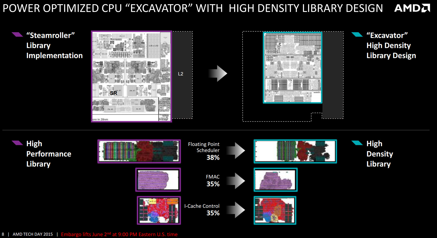
From a design perspective, Carrizo is the biggest departure to AMD’s APU line since the introduction of Bulldozer cores. While the underlying principle of two INT pipes and a shared FP pipe between dual schedulers is still present, the fundamental design behind the cores, the caches and the libraries have all changed. Part of this was covered at ISSCC, which we will also revisit here.
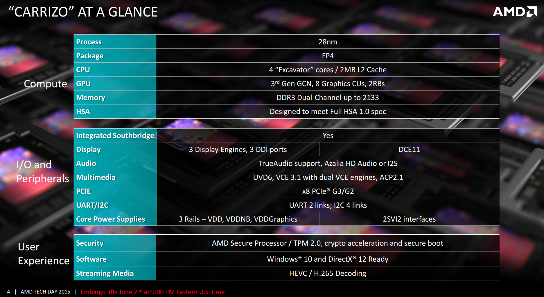
On a high level, Carrizo will be made at the 28nm node using a similar silicon tapered metal stack more akin to a GPU design rather than a CPU design. The new FP4 package will be used, but this will be shared with Carrizo-L, the new but currently unreleased lower-powered ‘Cat’ core based platform that will play in similar markets for lower cost systems. The two FP4 models are designed to be almost plug-and-play, simplifying designs for OEMs. All Carrizo APUs currently have four Excavator cores, more commonly referred to as a dual module design, and as a result the overall design will have 2MB of L2 cache.
Each Carrizo APU will feature AMD’s Graphics Core Next 1.2 architecture, listed above as 3rd Gen GCN, with up to 512 streaming processors in the top end design. Memory will still be dual channel, but at DDR3-2133. As noted in the previous slides where AMD tested on DDR3-1600, probing the memory power draw and seeing what OEMs decide to use an important aspect we wish to test. In terms of compute, AMD states that Carrizo is designed to meet the full HSA 1.0 specification as was released earlier this year. Barring any significant deviations in the specification, AMD expects Carrizo to be certified when the final version is ratified.
Carrizo integrates the southbridge/IO hub into the silicon design of the die itself, rather than a separate on package design. This brings the southbridge down from 40nm+ to 28nm, saving power and reducing long distance wires between the processor and the IO hub. This also allows the CPU to control the voltage and frequency of the southbridge more than before, offering further potential power saving improvements. Carrizo will also support three displays, allowing for potentially interesting combinations when it comes to more office oriented products and docks. TrueAudio is also present, although the number of titles that support it is few and the quality of both audio codecs and laptop speakers leaves a lot to be desired. Hopefully we will see the TrueAudio DSP opened up in an SDK at some point, allowing more than just specific developers to work with it.
External graphics is supported by a PCIe 3.0 x8 interface, and the system relies on three main rails for voltage across the SoC which allows for separate voltage binning of each of the parts. AMD’s Secure Processor, with cryptography acceleration, secure boot and BitLocker support are all in the mix.


137 Comments
View All Comments
Novacius - Tuesday, June 2, 2015 - link
From the article: "However for a 15W part, to which Carrizo will be primarily, this means either a 10%+ power reduction at the same frequency or a 5% increase in frequency for the same power. Should AMD release other APUs in the 7.5W region, this is where most of the gains are."It's power per core pair (module) and Carrizo clearly has two of them. This means the highest gains are exactly in the 15W TDP range.
Ian Cutress - Tuesday, June 2, 2015 - link
Good point, article updated :)Novacius - Tuesday, June 2, 2015 - link
"The big upgrade in graphics for Carrizo is that the maximum number of compute units for a mobile APU moves up from six (384 SPs) to eight (512 SPs), affording a 33% potential improvement."Mobile Kaveri already has 8 CUs (FX-7600P), but only at 35W.
el etro - Tuesday, June 2, 2015 - link
They stated that the power savings allowed them to put the 512SPs/8CUs in the 15W part.Ian Cutress - Wednesday, June 3, 2015 - link
I changed that on the fly a little while back between meetings, should be OK now :)ClamShall - Tuesday, June 2, 2015 - link
This article is basically just an explanation of AMD's marketing slides without actual empirical data to back things up (other than what has been provided by AMD). Worse still, it doesn't make any notable attempt to critically analyze whether the company's claims will or will not materialize.In short, this article should've been left to AMD's marketing team and posted on the company's site.
Iketh - Tuesday, June 2, 2015 - link
I don't have time to visit multiple sites. This is the only one I visit. Thank you AT for this article and keep them coming please.KenLuskin - Wednesday, June 3, 2015 - link
clamboy, This is a good article, and you are just another Intel fanboy with butt hurt. Intel does the EXACT same thing, and yet dumbos like you suck it up...... Bend over and assume the position for maximum penetration!SolMiester - Wednesday, June 3, 2015 - link
Eh?, and how are AMD providing the butt hurt?....formulav8 - Sunday, June 7, 2015 - link
Because there are many wackos who feels like an Intel/NVidia Corp is their mommy and hates to see AMD improve anything. Look at comments for Freesync reviews and such. Stupid how anyone gets attached to a Corp who cares nothing about you.