Intel’s Itanium Takes One Last Breath: Itanium 9700 Series CPUs Released
by Ian Cutress on May 11, 2017 11:10 AM EST- Posted in
- CPUs
- Intel
- Itanium
- Enterprise
- Enterprise CPUs
- IA-64
- Kittson
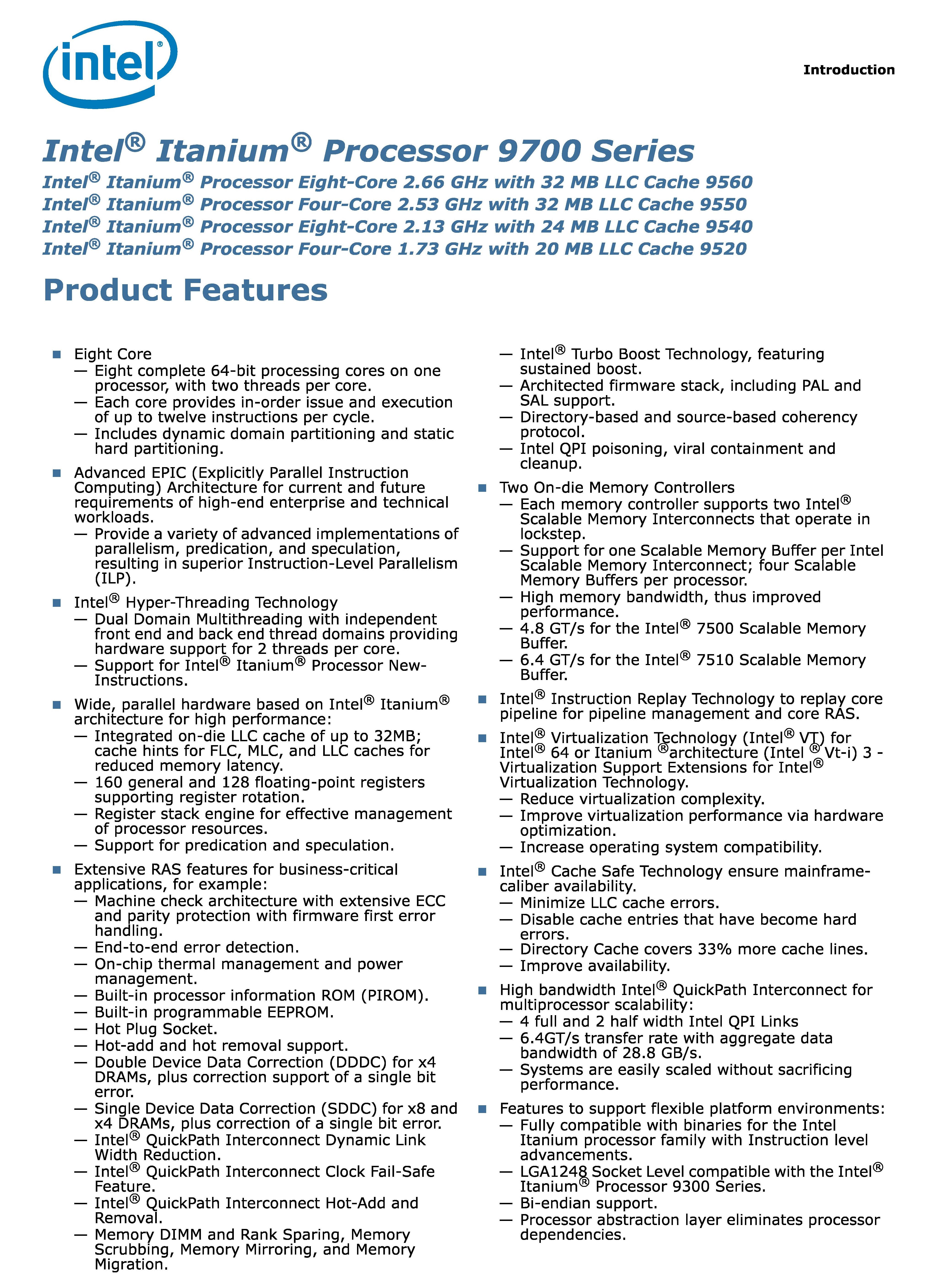
One of Intel’s ventures into the historic mainframe space was Itanium: a 64-bit capable processor designed in conjunction with Hewlett Packard. The main reason for Itanium was to run HP-UX and compete against big names, such as Oracle, using a new IA-64 instruction set. The appeal for the original Itanium parts was support for RAS features, ECC, and cores focus on a wide, parallel architecture - the latest cores support 12-wide execution for example. For a short while, there was success: HP’s systems based on Itanium are advertised as high-uptime mission critical servers, and a number of customers cling to these systems like a child clings to their favorite blanket due to the way they are integrated at the core of the company. The main purpose was to compete against other mission critical servers and mainframes based on SPARC and IBM Power.
So when the processors were initially delivered to customers, there was potential. However the initial impression was not great - they consumed too much power, were noisy, and needed over the top cooling. Over the years and generations of Itanium, the march into the x86 enterprise space with x86-64 drew potential Itanium customers away, then followed the drop of Microsoft's support for Itanium in 2008, and Oracle's dropped support in 2011. Xeon offerings were becoming popular, with CPUs incorporating the RAS/ECC features required, and Intel decided to slow down Itanium development as a result. In the meantime, due to the way the market was moving, HP transitioned a good part of its product stack to Xeons. Despite this, legal battles between HP and Oracle ensued given predicted support for HP-UX customers. At this point, there were fewer potential Itanium customers each quarter, although existing customers required support.
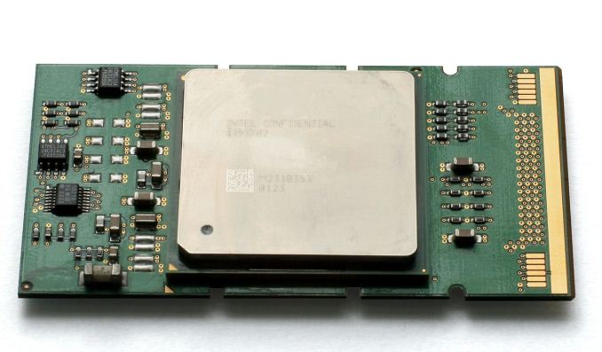
Today marks the release of the final known variant of Itanium, the 9700 series, beyond assurance testing. Intel spoke to IDG, stating that this generation, code-named Kittson, would be the final member of the Itanium family. These chips are likely to only end up in HP-based Integrity i6 high-uptime servers running HP-UX, and start at $14500. Hewlett Packard Enterprise has stated previously that it will keep support for Itanium-based products until 2025, with the latest OS update (HP-UX 11i v3 2017) coming in June.
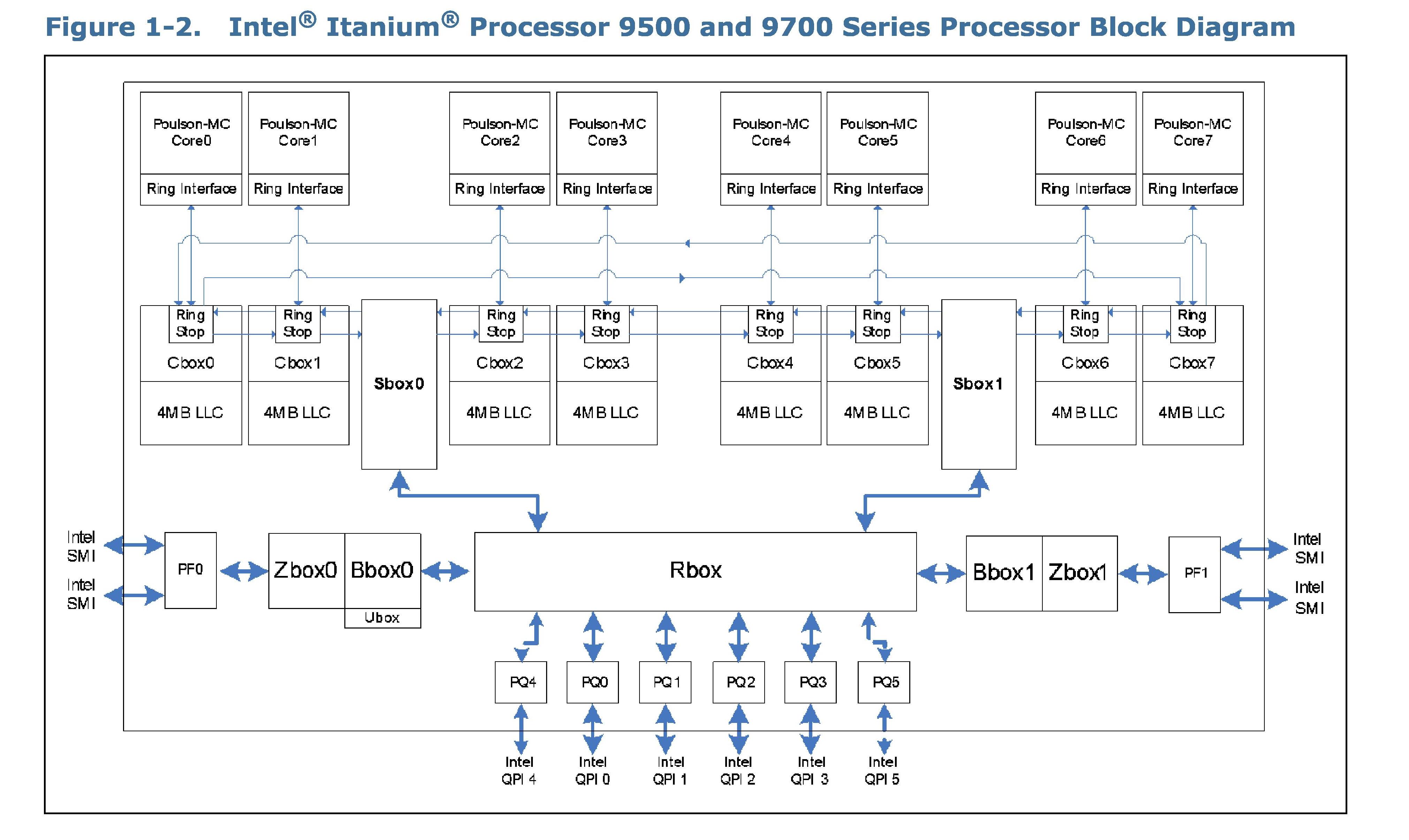
As for the processors themselves, four 9700 processors form the stack, with quad-core and eight-core parts all with hyperthreading, differing in frequency, power, and L3 cache.
| Intel Itanium (Kittson) CPUs | |||||
| Cores/ Threads |
Base Freq |
L3 | TDP | Cost* | |
| Itanium 9760 | 8/16 | 2.66 GHz | 32 MB | 170 W | $4650 |
| Itanium 9750 | 4/8 | 2.53 GHz | 32MB | 170W | $3750 |
| Itanium 9740 | 8/16 | 2.13 GHz | 24 MB | 170 W | $2650 |
| Itanium 9720 | 4/8 | 1.73 GHz | 20 MB | 130 W | $1350 |
*Cost is listed for the equivalent Poulson CPUs.
The base silicon comes in at 3.1 billion transistors, and are made on Intel’s 32nm process. Memory is supported up to DDR3-1067, with two memory controllers but support for scalable memory buffers is present. This is similar to the 9500 series, code-named Paulson. These chips are designed to be purely a drop into previous systems. Intel isn’t announcing an official press release around this, and unlike other ‘new architectures’, there are next to zero improvements. According to the documents, the only change is that the top two SKUs get a clock bump:
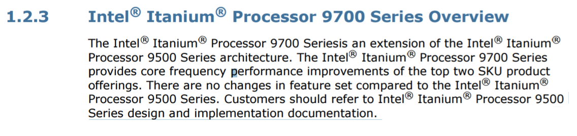
There’s probably something new under the hood, perhaps for a specific end-customer, but at this time Intel is directing anything 9700 related to equate to the 9500 series. Customers still interested in Itanium are directed to HPE resellers.
Carousel Image from Konstantin Lanzet (Wikipedia) of Itanium 2 (Poulson)
News Source: IDG


50 Comments
View All Comments
XabanakFanatik - Thursday, May 11, 2017 - link
Interesting how the Introduction document header says 9700 series, but the list of models beneath are all 95xx models. Document typo?Ian Cutress - Thursday, May 11, 2017 - link
Parts of the document that mention the 9700 all seem to be copy paste of the 9500 sections.LauRoman - Thursday, May 11, 2017 - link
I understand that it's an old architecture meant for some entities that smehow haven't moved off Itanium. Even if we forget the cost... 130W tdp for a quad core 1.73 ghz?SarahKerrigan - Thursday, May 11, 2017 - link
A lot of the TDP is the uncore needed to support 8-socket glueless SMP.mczak - Thursday, May 11, 2017 - link
I'd guess the actual power consumption is probably much lower (because the TDP compared to the much higher clocked, twice the core count versions is really incredibly high).Nevertheless, this is built on a 32nm process - you're not going to win any efficiency benchmarks using that... intel is lucky to still have a manufacturing plant for these new chips ;-).
DanNeely - Thursday, May 11, 2017 - link
Old fabs live for several generations past when they stop being state of the art. For Intel it's mostly chipsets and (I'm assuming) network adapters.mczak - Thursday, May 11, 2017 - link
Yeah I know that was just a joke (by the looks of it, intel operates fabs back to 65nm).But just to put this in context, Ivy Bridge (built on a 22nm process) was released nearly exactly 5 years ago. The last "big core" x86 chips built on 32nm was Sandy Bridge over 6 years ago.
StevoLincolnite - Friday, May 12, 2017 - link
There were Pentium 4 chips built at 65nm... And the Interposer for High Bandwidth Memory was built at 65nm.mode_13h - Friday, May 12, 2017 - link
Yeah, I was hoping 65 nm might be enough for Pescott to stretch its legs and hit the kind of clock speeds for which it was architected. Sadly, it was not.Kevin G - Friday, May 12, 2017 - link
Intel moved their chipsets to state-of-the-art processes around the time of Sandy/Ivy Bridge. This was to cut platform power for mobile systems. This is one reason how they have been able to produce 5W system packages for the Y series. It does look like Intel will not be as aggressive with this in the future due to difficulties of the newer nodes. The cost/benefit isn't there to migrate chipsets to a new node when they immediately come online but should sync when volume ramps up (they should be on the same node for Intel's 'architecture' and 'optimize' phase.)The network adapters is true to an extent. Some of the high speed 100 Gbit equipment is kept on the newest process for both power consumption and performance concerns. While not state of the art in a raw transistor size sense, Intel does have a production silicon phonotics line going right now. That line is reportedly being used for transceiver chips for both Intel and Cisco. However, there are plenty of 1 Gbit and some 10 Gbit equipment that Intel makes on their old fabs. Intel's wireless chips are spread across a mix of nodes to balance performance, analog logic and power consumption factors. They also absorbed Texas Instrument's cable modem business a few years ago but there hasn't been enough time for products in that portfolio to be migrated to Intel's own fabs. It is not expected that those chips will receive aggressive treatment on the manufacturing side.
The scalable memory buffers for a time were kept a generation behind intentionally as they have some of the highest speed circuits Intel has devised internally in a chip (6.4 Ghz). Ironically, these are still used with the Itanium 9700. I suspect that the new memory buffers used in recent Xeon E7's have migrated to a new node as the link design has radically changed (originally it requires internal logic running at six times the base memory clock. 1067 Mhz -> 6.4 Ghz logic).