MRAM Developer Day, IBM Keynote Live Blog
by Ian Cutress on August 6, 2018 1:17 PM EST- Posted in
- Memory
- Storage
- Trade Shows
- Live Blog
- MRAM
- MRAM Developer Day
- FMS 2018

01:19PM EDT - Third Keynote in this session is from IBM Research: STT-MRAM is Ready for Applications Today.
01:21PM EDT - In a bit, Discussing the MRAM in IBM FlashCore, a currently available product
01:21PM EDT - Starting with data about STT-MRAM with Samsung

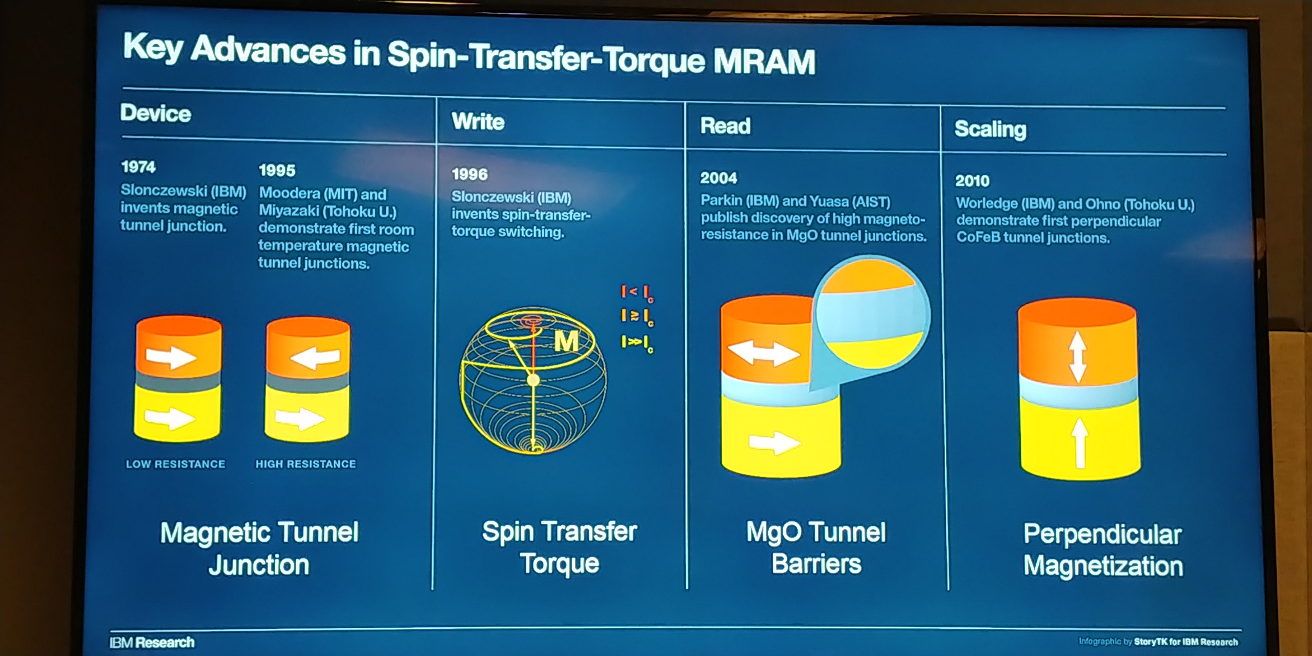
01:22PM EDT - Slonczewski invented STT in 1996. He developed the magnetic tunnel junction in 1974
01:22PM EDT - 2004 developed the MgO tunnel barrier for reading
01:23PM EDT - 2010 Developed perpendicular CoFeB tunnel junctions to make the technology scale
01:23PM EDT - Perpendicular is how all devices are used today

01:23PM EDT - MRAM Applications - Standalone, Embedded, Cache
01:23PM EDT - MRAM is unlikely to replace DRAM any time soon - DRAM is still scaling
01:24PM EDT - Perfect applications are battery backed SRAM, or buffers for storage
01:24PM EDT - Using MRAM to replace embedded flash in MCUs
01:24PM EDT - eFlash doesn't scale below 20nm
01:25PM EDT - Need a 400C process required to enable it
01:25PM EDT - A couple of years ago, new materials were discovered to make this less of an issue
01:25PM EDT - Using MRAM to replace L3 cache - replacement to eDRAM
01:26PM EDT - 400C process, 4-256 megabit, 1-2ns read/write, unlimited endurance
01:26PM EDT - Also mobile and embedded. The 'Killer' app for MRAM. Replacing low speed SRAM
01:27PM EDT - Use co-processor when in sleep using MRAM for low power
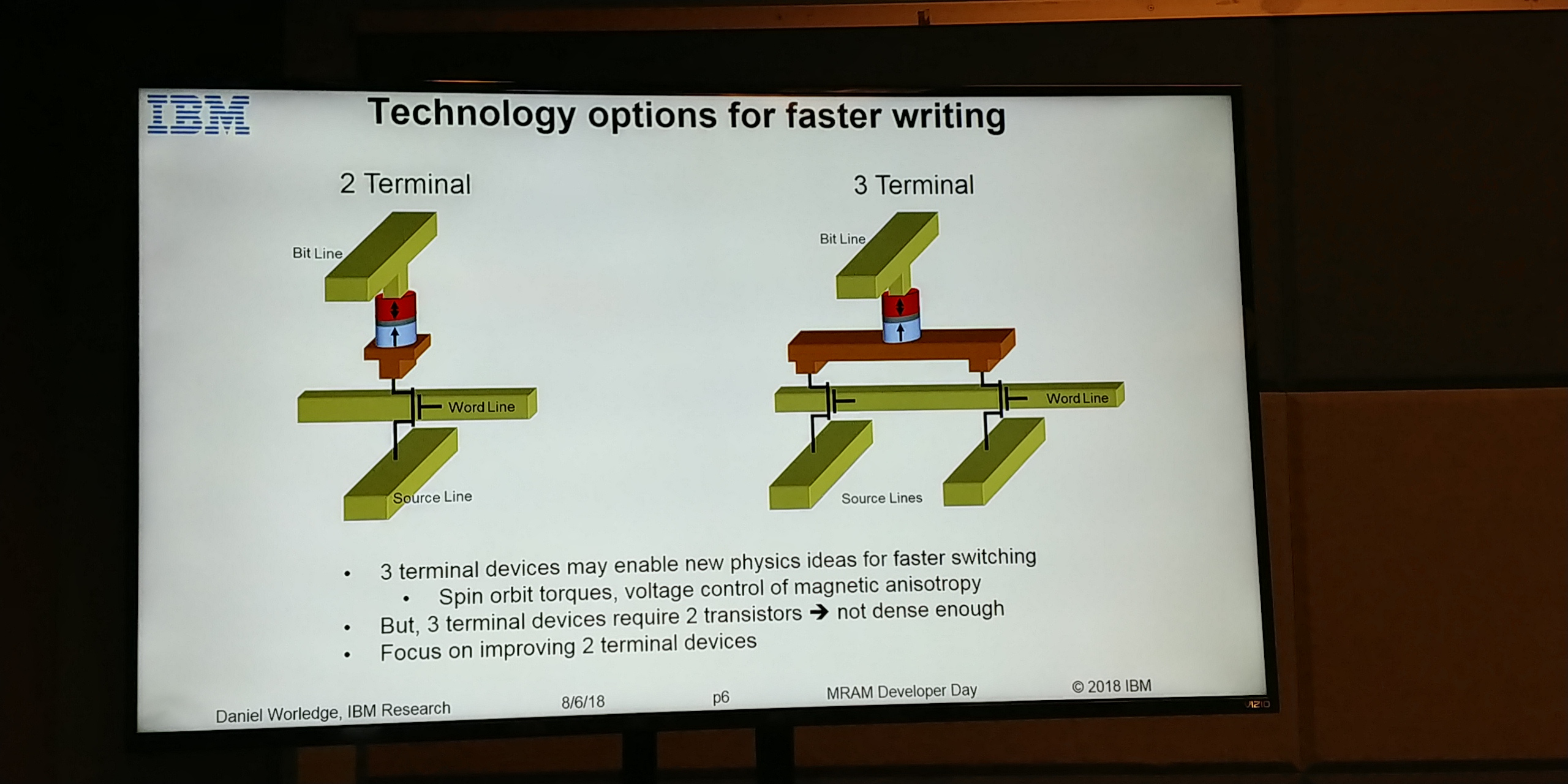
01:28PM EDT - Normal MRAM device today is a 2-terminal device. MRAM cell has one transistors.
01:28PM EDT - Looking at 3-terminal devices. New physics ideas can be explored with this type of devices. Spin-Hall effects etc
01:28PM EDT - Other ideas such as voltage control, such as anisotrophy
01:29PM EDT - Downside is losing density, and with memory density is king
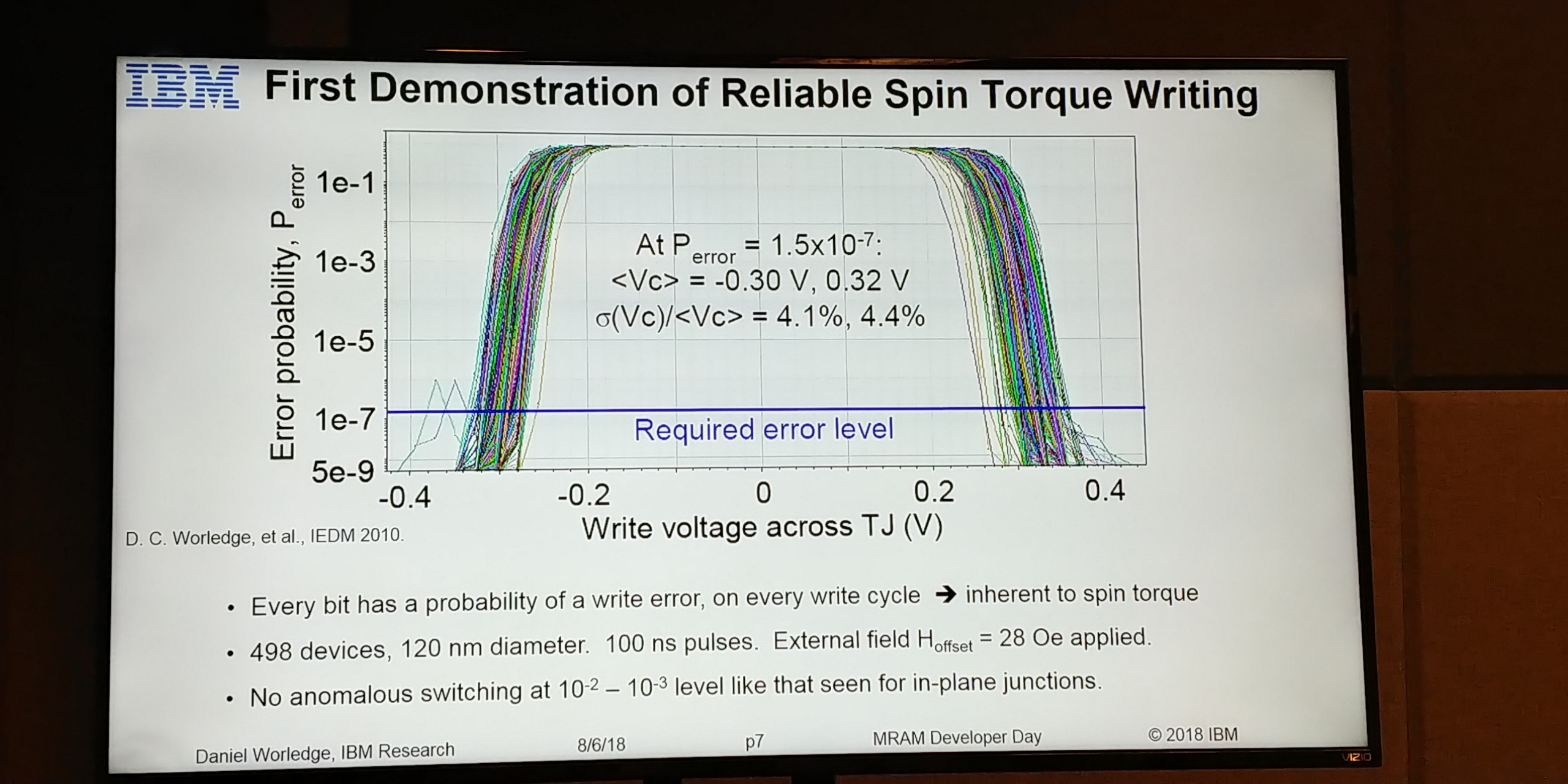
01:30PM EDT - Curves are called write-error curves. Error probability vs voltage vias
01:30PM EDT - bias
01:30PM EDT - STT has inherently error rate for bit writing
01:32PM EDT - Has to increase voltage in order to ensure that bit is written - because bias is applied in equilibrium and waiting for thermal effects to knock it out of equilibrium
01:32PM EDT - That data was 120nm with 100ns pulse
01:32PM EDT - Can now show 39nm with 10ns pulses
01:32PM EDT - For MRAM, 10ns is now possible
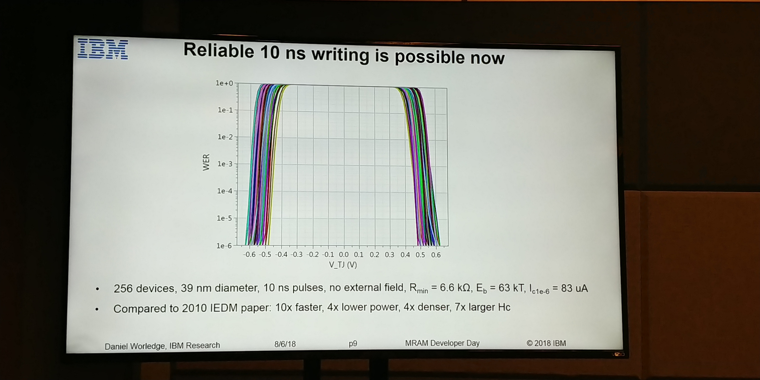
01:32PM EDT - Compared to 2010: 10x faster, 4x lower power, 4x denser
01:33PM EDT - Below 5ns is tough with 2-terminal
01:33PM EDT - On scaling, can junctions as small as 11nm
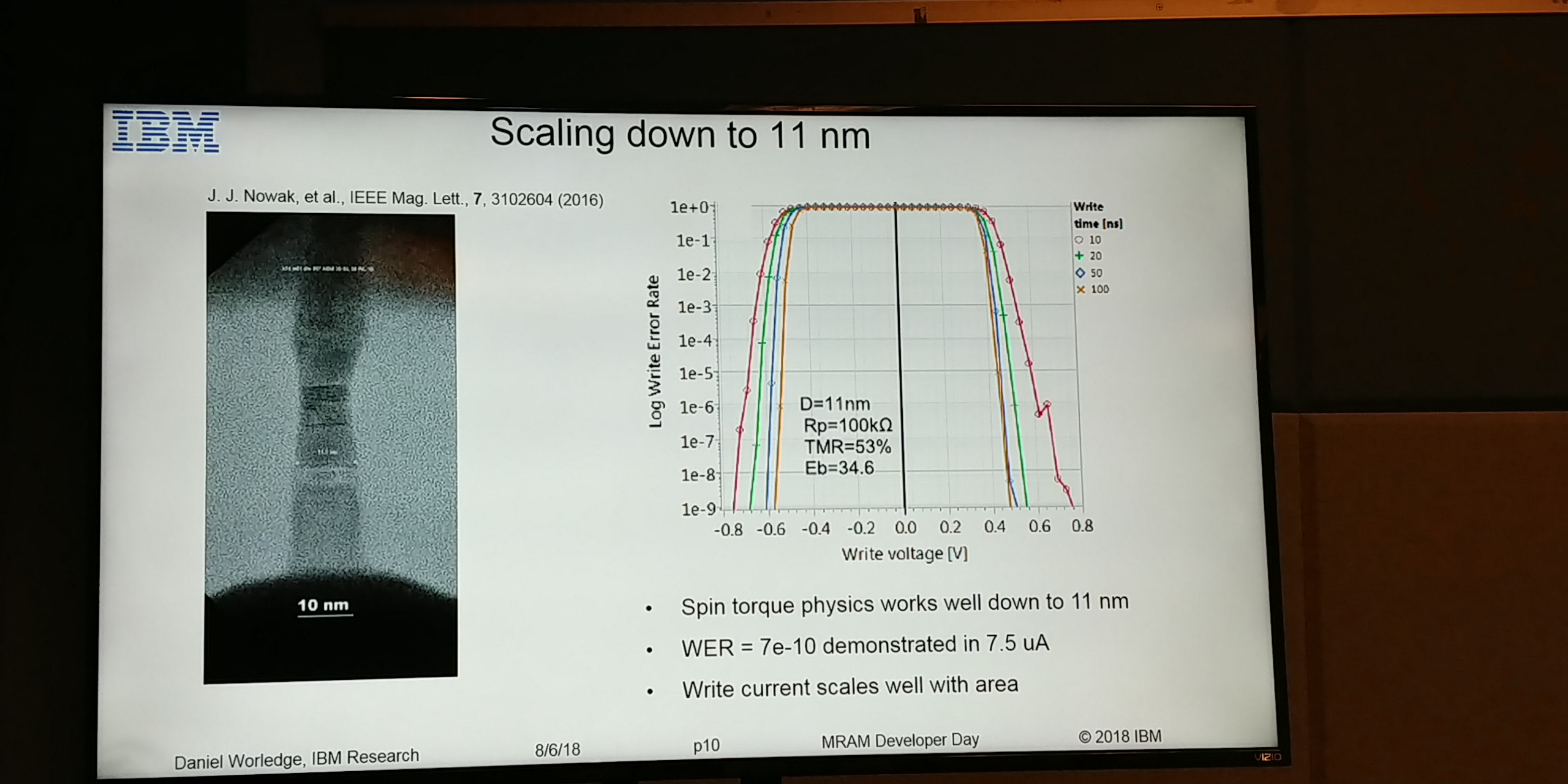
01:33PM EDT - Current in MRAM scales with area
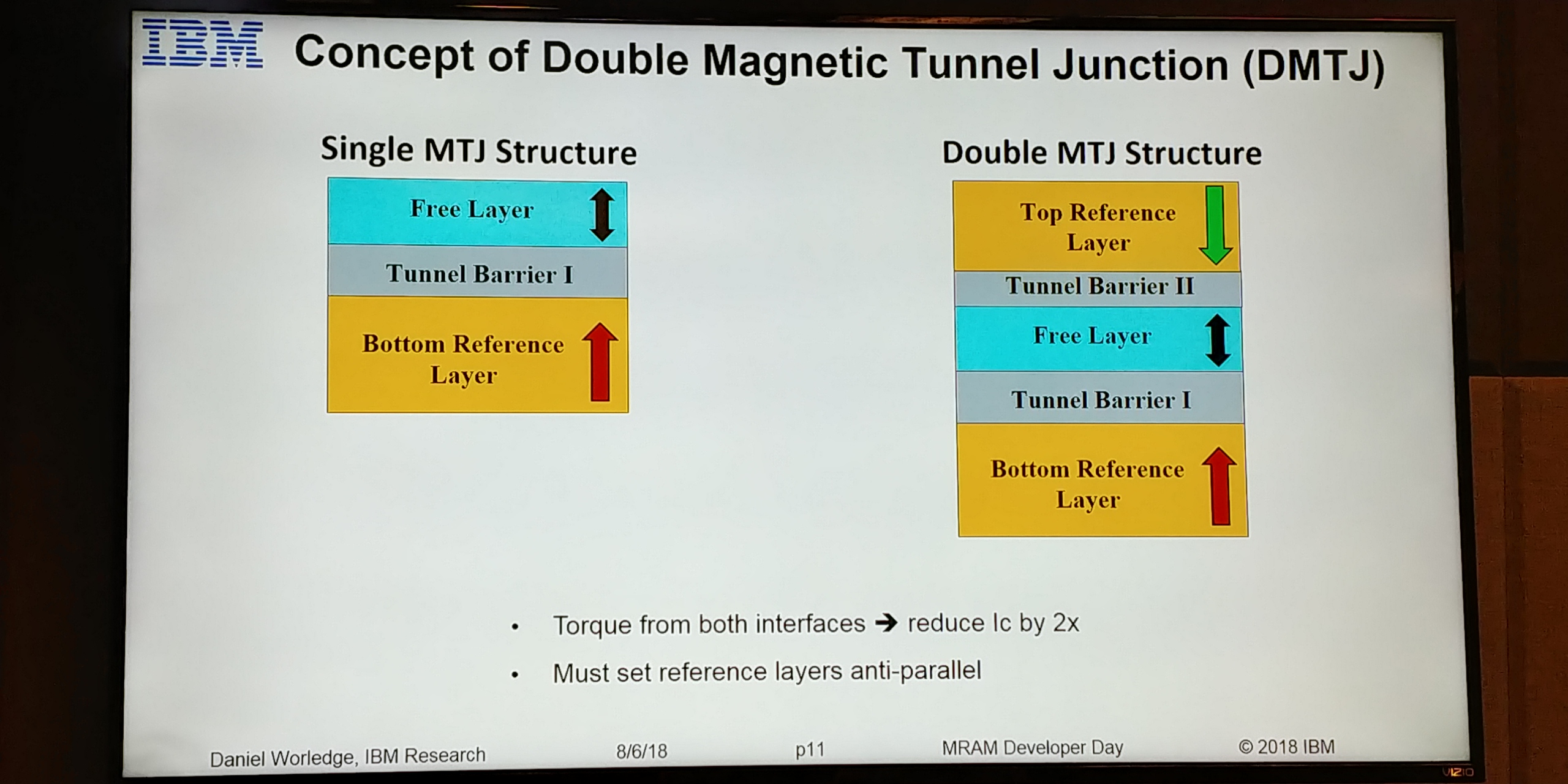
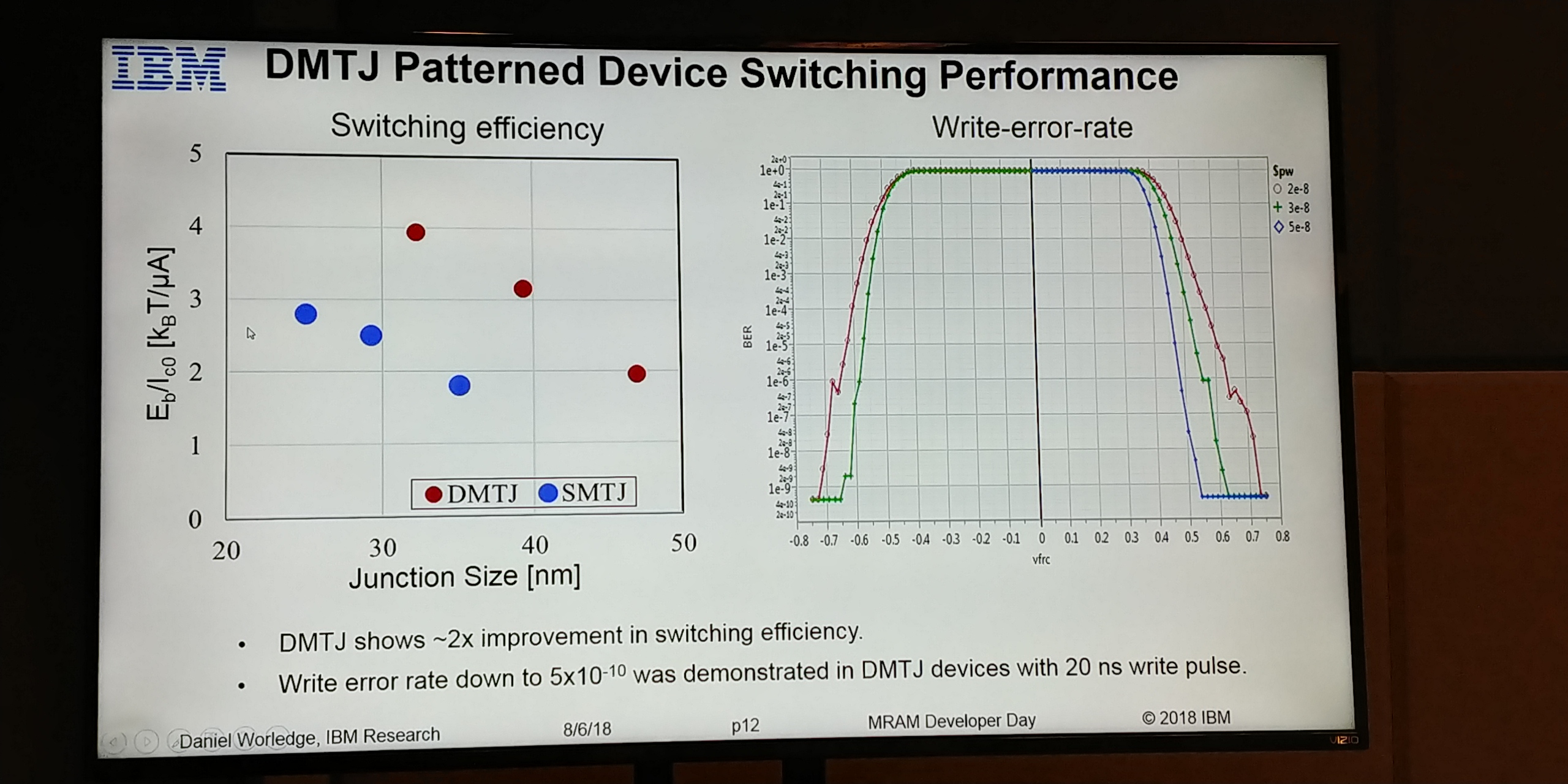
01:34PM EDT - Ideas for future development include two reference layers
01:34PM EDT - reduce current by half
01:34PM EDT - MTJ = magnetic tunnel junction
01:35PM EDT - A more complicated structure, but not ready for products today. Perhaps in 5 years
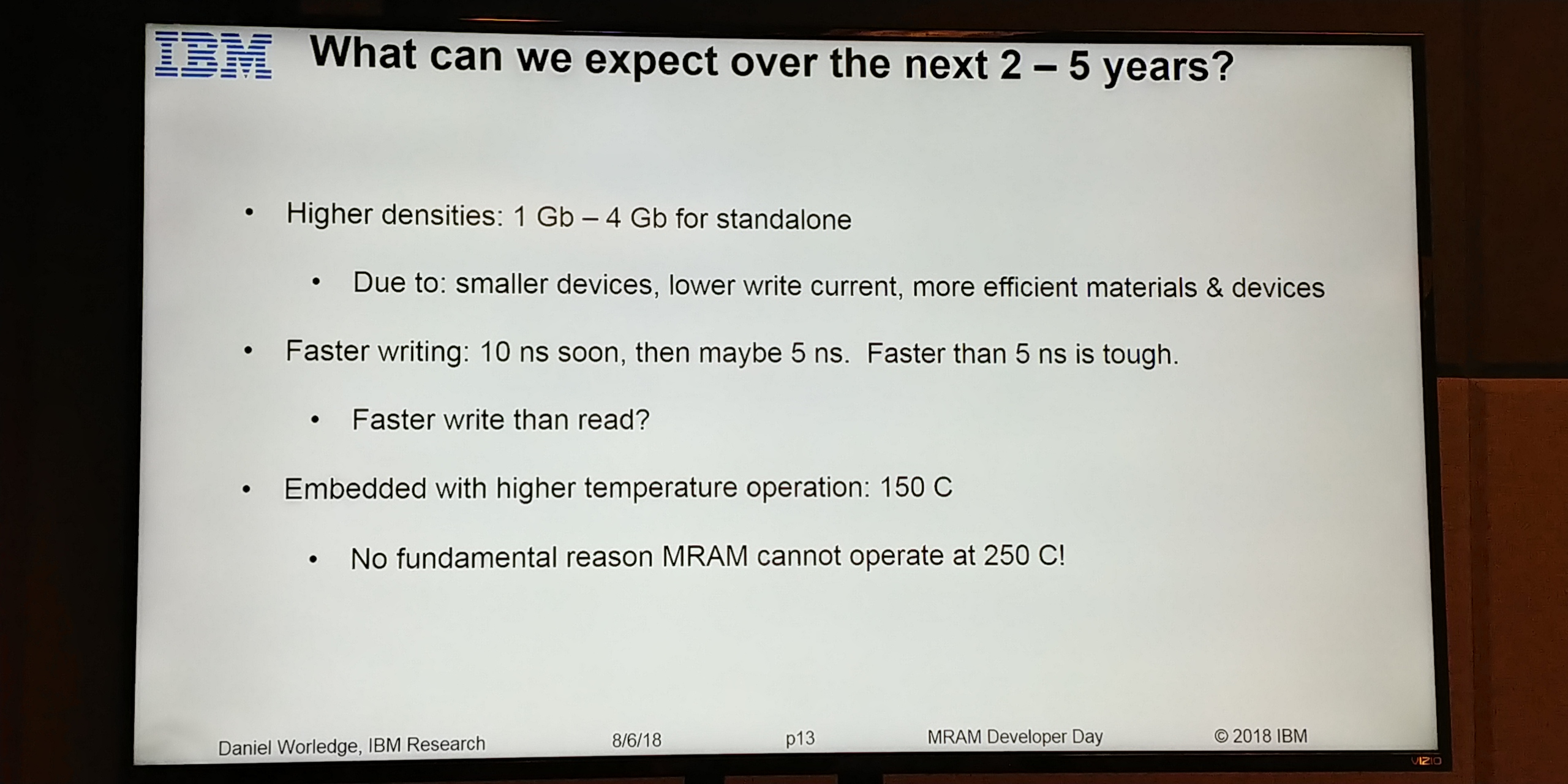
01:35PM EDT - Over next 2-5 years, main gain is going to be density
01:35PM EDT - Smaller devices, lower write current, more efficient materials
01:35PM EDT - Faster writing as well. Current products are 30-50ns pulses, expect 10ns soon (1-2 years), maybe 5ns in 5 years
01:36PM EDT - Can write faster than reading with 3 tunnel devices
01:37PM EDT - Current spec for 125C operation, 150C will be coming soon. No fundamental reason why MRAM can't operate at 250C.
01:37PM EDT - The tradeoff is that the device has to be hardened at a level of drive currents to enable writes
01:37PM EDT - Now talking about IBM devices using MRAM
01:38PM EDT - FlashCore
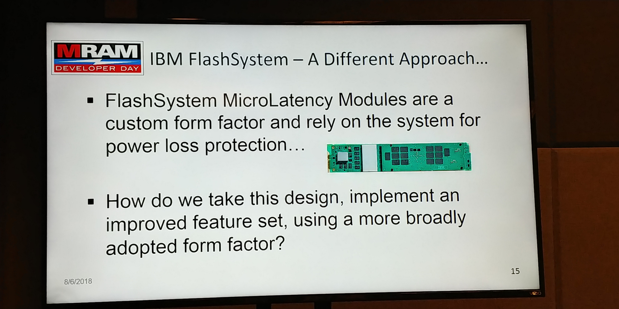
01:38PM EDT - Design custom size solutions with FlashSystem
01:38PM EDT - 70mm height, 250-260mm depth
01:39PM EDT - Recent designs (Nov 2017) shows an 18TB module in that size
01:39PM EDT - Next question is how to embed this in other applications. The problem is the custom design though
01:39PM EDT - E.g. the custom form factor left the power control on the system. To scale out to other use cases, need to manage it locally
01:40PM EDT - Enabling this for a common form factor
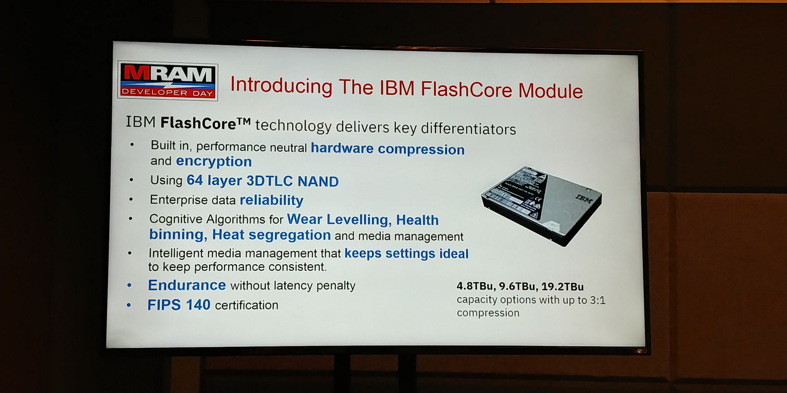
01:40PM EDT - Moving the long card into a 2.5-inch 15mm form factor
01:41PM EDT - 19.2 TB in a 2.5-inch
01:41PM EDT - Taking a 3 FPGA design from the card into one FPGA
01:41PM EDT - Two years ago we started speaking to Everspin about MRAM
01:42PM EDT - MRAM is a cornerstone to this new drive
01:42PM EDT - Not having to do DRAM to NAND
01:42PM EDT - Started with compnoent level qualification
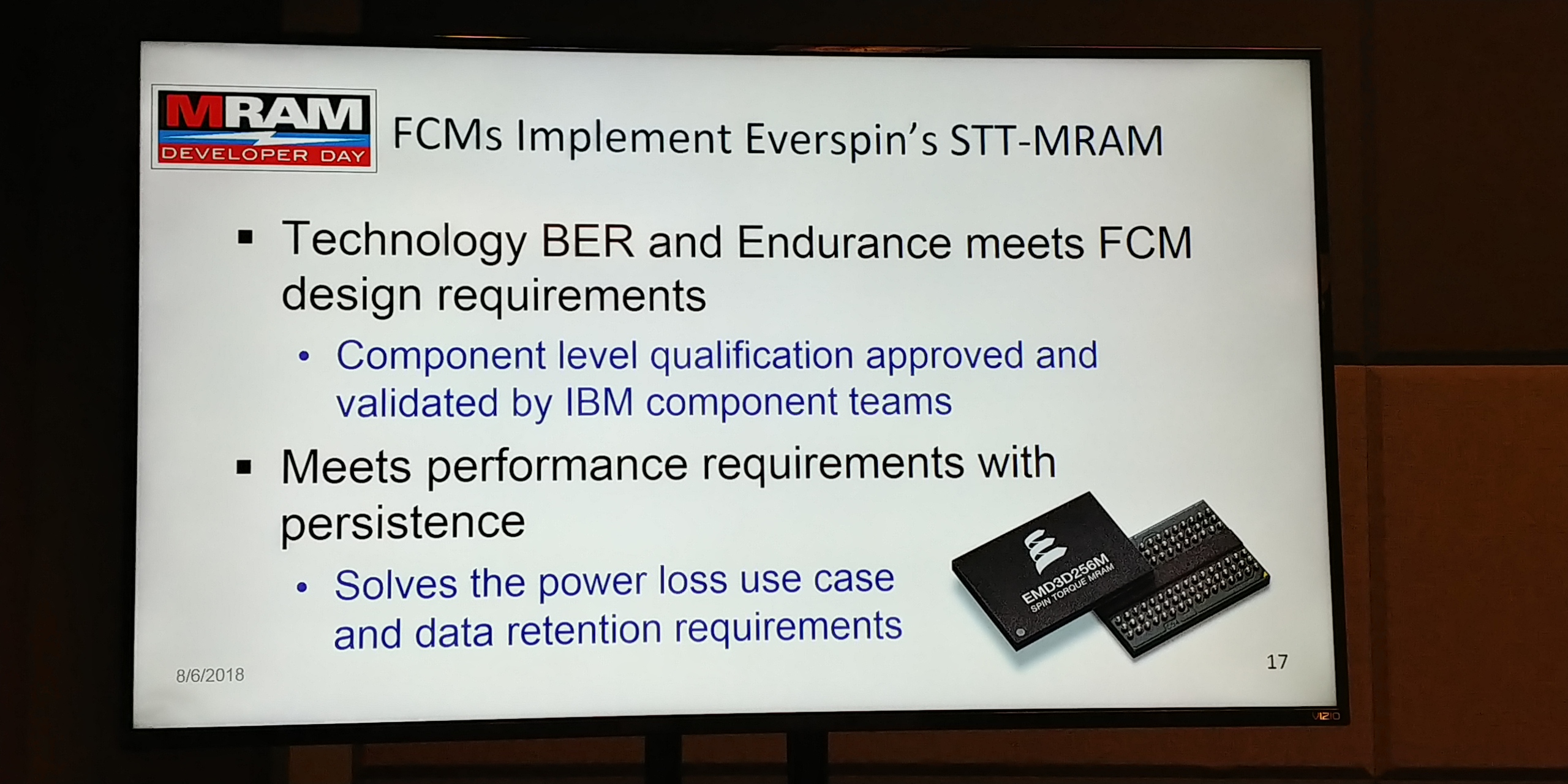
01:43PM EDT - It all worked - shipping drives to customers in October
01:43PM EDT - Didn't have enough space for supercaps for the high-power FPGA to commit data
01:43PM EDT - New design has no supercaps by using MRAM
01:44PM EDT - Using a Xilinx FPGA
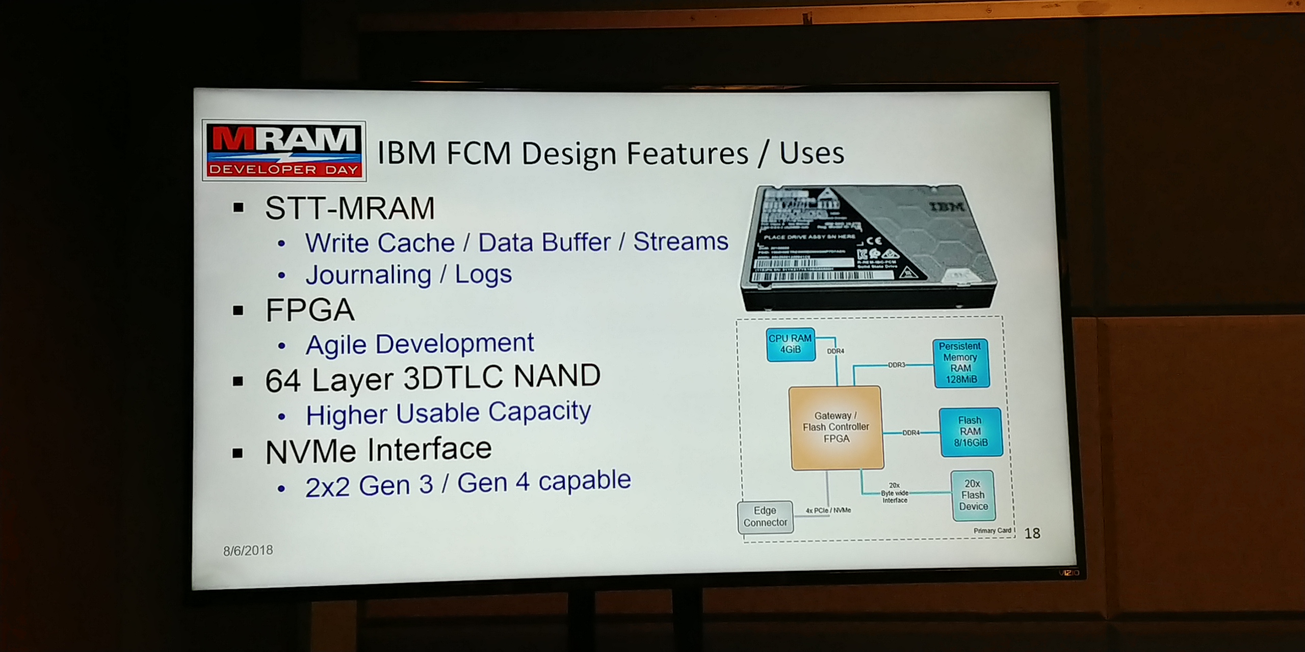
01:44PM EDT - Design allows the write stream to be compressed into MRAM
01:45PM EDT - Power failure allows the system to harden the MRAM to enable commit at next power on
01:45PM EDT - FPGA has 4GiB of DDR4, 128 MiB of Persistent DDR3, and 8GiB of Flash DDR4 for the FPGA
01:46PM EDT - 2x2 Gen 3.0 NVMe interface. Gen 4.0 capable
01:46PM EDT - No details on IOPS or R/W data
01:47PM EDT - Moving to the MRAM wasn't as big as a change to the architecture as expected
01:47PM EDT - Hyper scaled - lots of low speed lanes
01:47PM EDT - 20-lane Flash interface
01:48PM EDT - Going forward, density of the MRAM is going to be key. 1Gb will allow some optimizations
01:49PM EDT - On the roadmap is to create a persistent memory region for NVMe
01:49PM EDT - Typically use DRAM today, would like to use the storage memory interface instead
01:49PM EDT - FPGA allows us to implement this if we can sort it, lots of potential in future technology
01:51PM EDT - FPGA is not on-the-fly reconfigurable, but firmware updates include updated RTL
01:52PM EDT - No significant impact into BOM cost for MRAM vs DRAM
01:53PM EDT - On the wishlist for MRAM is endurance, better error rate (the device has ECC engines to help), then capacity
01:55PM EDT - That's a wrap!


0 Comments
View All Comments