Intel’s New eASIC N5X Series: Hardened Security for 5G and AI Through Structured ASICs
by Dr. Ian Cutress on November 24, 2020 11:00 AM EST
The programmability of a processor is a scale is all about flexibility and performance – something highly programmable and customizable is adaptable to all sort of situations, but often isn’t as fast. However, something that has a very specified compute pathway can go very fast, but can’t do much beyond that pathway. On the flexible side, we have FPGAs, that can be configured to do almost anything. On the fixed side, we have ASICs, such as fixed function hardware for AI. Somewhere in the middle is what’s called a ‘Structured ASIC’, which tries to combine as many benefits from the two.
An FPGA, or Field Programmable Gate Array, is a piece of silicon built that can be configured after manufacturing. By implementing a series of programmable logic blocks, memory cells, and layers of connectivity, a programmer with enough knowledge can configure the FPGA to run the equivalent of unique circuit designs for specific functions. For example, any series of AI calculations can be done on a CPU core slowly, and a subset of them can be very fast on a GPU, but if that calculation methodology has to change, the FPGA can be adjusted to be GPU-like of efficiency while being as configurable as the CPU.
An ASIC, by contrast, is a very fixed unit of hardware. By knowing what sort of calculations are expected, an ASIC can implement those calculations very fast and very efficiently, but it can only do that sort of calculation. For example, a graphics card can be thought of as an ASIC, as it does graphics very well, however the special 4K decode engine inside the GPU is better suited to the term of an ASIC, because all it does is decode 4K images/video and it knows how to do it much faster and much more efficiently than a CPU or an FPGA could.
Obviously if there are security concerns, an FPGA has the ability to perhaps be configured to avoid that issue. An ASIC by contrast has no solution. FPGAs can be deployed with updates to be sent later, whereas ASICs cannot be updated. FPGAs are initially very cheap, and ASICs require a lot of up-front non-reusable engineering (NRE) costs, however when built at scale, can offer something cheaper at orders of magnitude lower power and higher performance. These are some of the trade-offs.
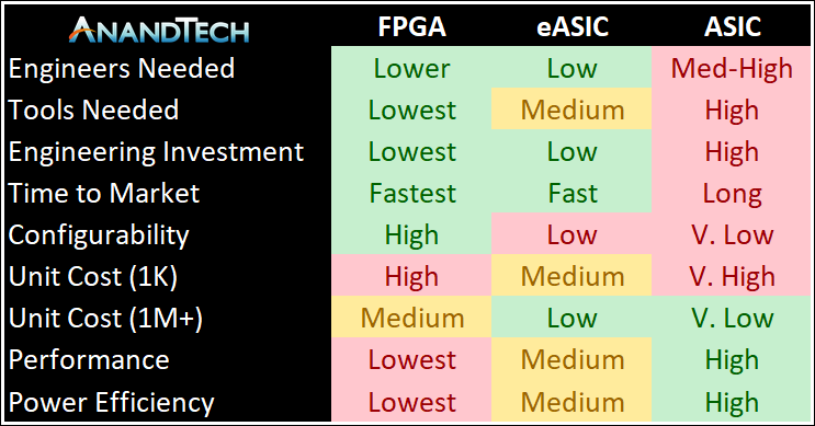
A structured ASIC (or for Intel, an eASIC), is something between the two. The underlying design of an eASIC product is similar to an FPGA, but by doing some small upfront NRE/circuit design, an eASIC company changes some of its silicon manufacturing masks for FPGAs for the design in question. This means that the eASIC is no longer as configurable as an FPGA as it now has some rigid pathways in its silicon, but it takes gains some of the performance and power efficiency by having rigid pathways. It also hasn’t required the large amount of design costs that a full ASIC requires, and thus saves a lot of cost, and the product ends up somewhere between an FPGA and an ASIC.
For any company interested in something like a structured ASIC, it means developing a relationship with a vendor offering a portfolio of structured ASIC base designs, and then implementing some level of circuit customization on top at the point of manufacture.
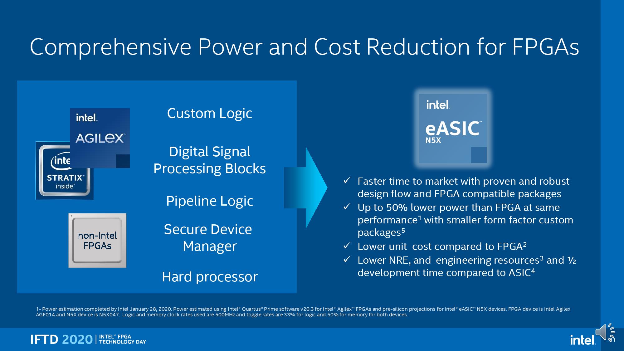
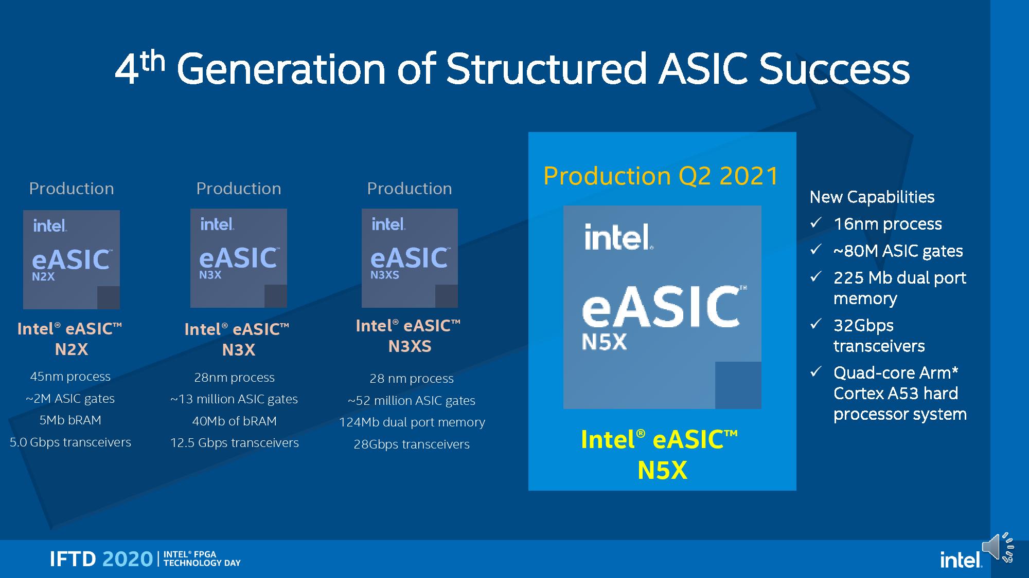
Intel recently purchased a company called eASIC in mid-2018 to do just this, and the first line of products are called the N5X eASICs (Diamond Mesa, for anyone following code names), which add-in hardened embedded CPU cores to allow for control and security. A number of technologies have been pulled in from the Intel Agilex FPGA family to improve the previous eASIC offering, as well as a software platform.
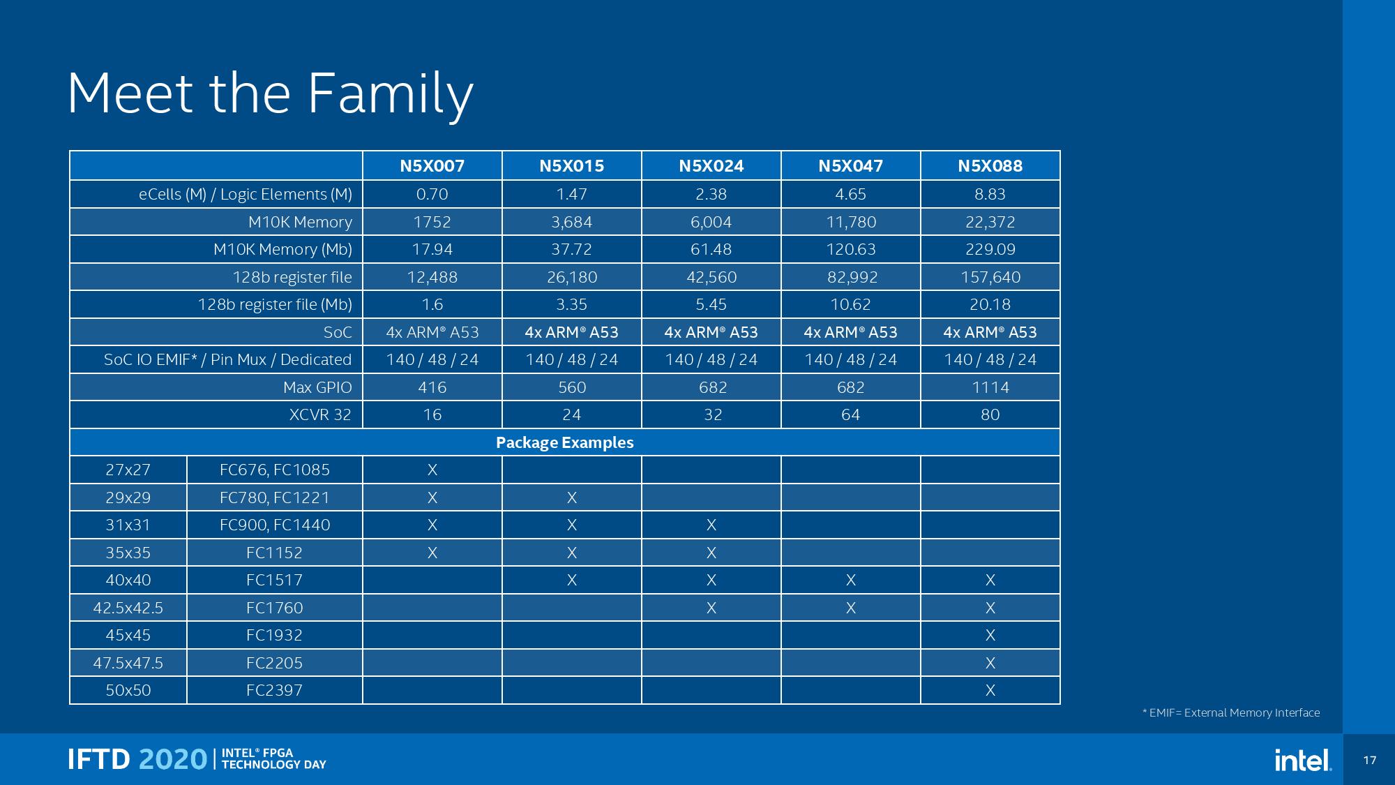
The N5X series base design is built on a 16nm process (TSMC, by virtue of the acquisition), uses up to 80 million eASIC gates (8.8 million FPGA-like look up tables/logic elements), 225 megabits of dual port memory, supports 32G transceiver tiles, and features a quad-core A53 hard processor system. The N5X product line is in the form of N5Xabc, where abc is the number of FPGA-equivalent cells divided by 100,000 – thus the top model is the N5X088, with 8.8 million.
With customers implementing their own DSPs and pipelines into the N5X, Intel is promising faster time-to-market than traditional ASICs, up to 50% lower power than FPGAs with smaller form factor packaging, overall lower unit cost than FPGAs, and enhanced security.
Intel decided to make this announcement at its FPGA Technology Day, which coincided directly with the annual Supercomputing conference. It seemed odd that Intel would cause the two to clash. The N5X family of products however won’t be in production until Q2 2021.
Intel did provide a slide showing what's actually inside one of its eASIC products:
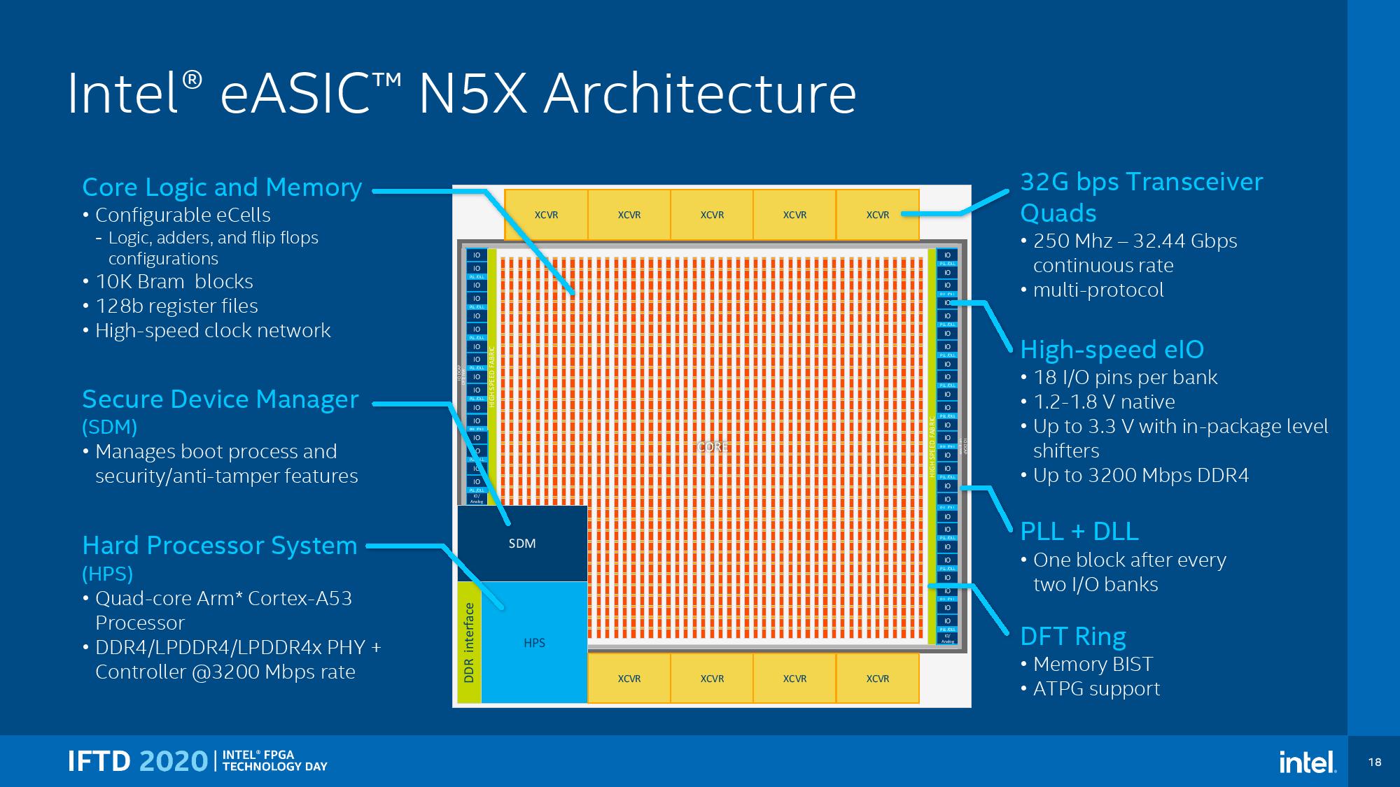
Source: Intel
Related Reading
- Intel To Acquire eASIC: Lower Cost ASICs in FPGA Design Time
- Intel’s EMIB Now Between Two High TDP Die: The New Stratix 10 GX 10M FPGA
- Intel Agilex: 10nm FPGAs with PCIe 5.0, DDR5, and CXL
- Bittware 4x100G FPGA Card, Uses Intel 10nm Agilex and oneAPI
- Xilinx Announces World Largest FPGA: Virtex Ultrascale+ VU19P with 9m Cells
- Intel Announces The FPGA PAC N3000 for 5G Networks


6 Comments
View All Comments
Duncan Macdonald - Tuesday, November 24, 2020 - link
One security concern is that the device CAN be reconfigured. An ASIC can not be changed after manufacture by malicious software - a FPGA or eASIC can be.A more accurate description would be that the ability to program the eASIC allows for correcting some design errors without the expense that producing a new ASIC would bring
ZolaIII - Wednesday, November 25, 2020 - link
Intel reinventing hot water again. There are flexible programmable DSP's which are available as licensable IP's. Some of which are very flexible like for instance recent generations Tensilica one's. They are certainly better choice & cheaper & should also still be more power efficient than this "eASIC".RSAUser - Wednesday, November 25, 2020 - link
Not sure how you already know this as it's not yet to market afaik.ZolaIII - Wednesday, November 25, 2020 - link
This has a programmable cell area (FPGA), DSD, couple of switches (ASIC's), quad cluster ARM A53, ram and a controller while it's made with 16 nm.Simply put i don't see reason for existence for this & it's not exactly built upon top teach either.
JayNor - Monday, November 30, 2020 - link
Intel's NNP-I inference chips include Tensilica Vision P6 DSPs.andychow - Friday, November 27, 2020 - link
Amazing they claim it's 4th generation, meanwhile it's going to be available the first time in 2021 right? I've searched the N2XLT190, can't find it anywhere.The only page I can find is https://www.intel.ca/content/www/ca/en/products/pr...
Which wayback machine shows me never existed before October 25th, 2020.
Even their name series (N2X, N3X, ..., N5X) seem to suggest it's a 5th gen product. What a crock of intel marketing.