EUV Pellicles Ready For Fabs, Expected to Boost Chip Yields and Sizes
by Anton Shilov on March 31, 2021 6:00 PM EST- Posted in
- Semiconductors
- EUV
- EUVL
- ASML
- TSMC
- Samsung Foundry
Foundries started limited usage of extreme ultraviolet (EUV) lithography for high-volume manufacturing (HVM) of chips in 2019. At the time, ASML's Twinscan NXE scanners were good enough for production, but the full EUV ecosystem was not quite there. One of the things that impacted EUV was the lack of protective pellicles for photomasks, which limited usage of EUV tools and affected yields. Fortunately, the situation with pellicles has finally improved thanks to the recent introduction of production-ready EUV pellicles, and matters promise to get even better in the coming years.
Protecting Precious Reticles
ASML has made a great progress with its Twinscan NXE EUV lithography tools in the recent years, improving performance of light source, availability time, and productivity. Its industry peers have also done a lot to make high-volume manufacturing (HVM) using EUV equipment possible. Still, the EUV ecosystem needs to develop further. One of the most notorious challenges the semiconductor supply chain faced with EUV is development of pellicles that were not available two years ago, which is why TSMC and Samsung Foundry had to invent ways how to use their EUV scanners without protective films.
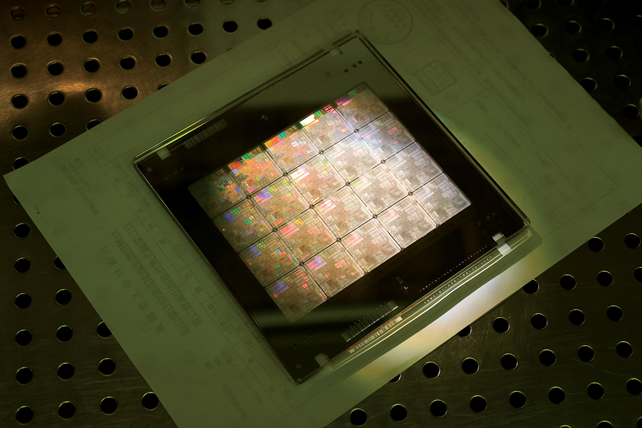
For Reference: A 16nm TSMC Pellicle With Reticle
Pellicles protect 6×6-inch photomasks (reticles) during the chip production flow by sealing them away from particles that could land on their surface, which would otherwise damage them or introduce defects to wafers in production. Each reticle for an EUV tool costs $300,000, so chipmakers are eager to protect them against damage by particles or even the EUV radiation itself as this lowers their costs. Meanwhile, reducing risks associated with yields is perhaps even more important.
The need for pellicles, in turn, varies depending on the manufacturer and the types of photomasks employed. Intel, which is known for its big CPU dies, tends to use single-die reticles, which means that just one mask defect introduced by a particle automatically kills the whole die. Meanwhile, if a 25-die photomask is used, a particle adder will 'only' result in 4% lower yield (one dead die), which is why it's been possible to get away without pellicles for smaller chips and multi-die photomasks.
ASML Leading the Pack. For Now
The industry started to develop protective films for EUV tools relatively late after it transpired that nobody can guarantee that an ultra-complex EUV scanner is 100% free of harmful particles, which is why they were not ready in 2019.
Pellicles for photomasks to be used with deep ultraviolet (DUV) lithography equipment are common and cheap. By contrast, since photomasks for EUV are different from photomasks for DUV (EUV masks are essentially 250 to 350-nm thick stacks featuring 40 to 50 alternating layers of silicon and molybdenum on a substrate), pellicles for such reticles are also quite different. In particular, the very short wavelength of EUV means that pellicles for it have a number of requirements that make them uneasy to produce and expensive. EUV pellicles have to be extremely thin, should not affect reflection characteristics of reticles, should feature a high transmission rate (the higher the rate, the higher is productivity of a scanner), should sustain high EUV power levels, and withstand extreme temperatures (from 600ºC to 1,000ºC in the future).
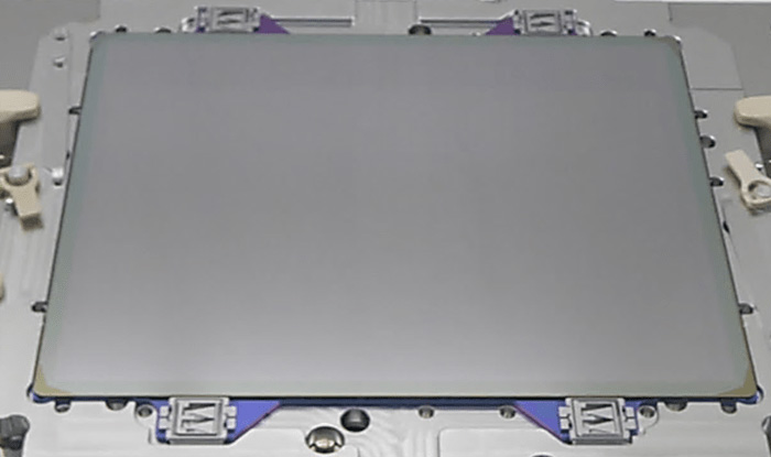
ASML's EUV Pellicle (Image Credit: Semiconductor Engineering)
"Most materials absorb very strongly at the more energetic 13.5nm EUV wavelength and, even when the most EUV-transparent materials are selected, the membranes must be extremely thin to approach 90% transmittance," said Emily Gallagher, a principal member of technical staff at Imec. "Such thin membranes are not usually capable of maintaining sufficient strength to be free-standing at the required dimensions. Additionally, the EUV scanner environment is not compatible with many materials and will subject the pellicle to pump-vent cycles."
To date, a number of EUV pellicle options have emerged, according to SemiEngineering:
- ASML introduced its first EUV pellicles in 2019 and licensed the technology to Mitsui Chemicals, which intends to start their volume sales in Q2 2021. Since then, ASML has improved its pellicles.
- Imec has disclosed test results of its pellicles based on carbon nanotubes.
- Graphene Square, Freudenberg Sealing Technologies (FST), and some universities are developing their own pellicles.
So far, only ASML has managed to create commercially viable pellicles for EUV tools that are actually available. ASML's pellicles are based on polysilicon that is 50 nm thick. Back in 2016, they demonstrated a 78% transmissions rate on a simulated 175W source. Currently ASML can sell a pellicle with an 88% transmission rate. And shortly, Mitsui will start supplying such pellicles in volume.
ASML's latest prototypes made of metal silicide demonstrate a 90.6% transmission rate with 0.2% non-uniformities and less than 0.005% reflectivity on a 400W source.
"This upgrade supports our roadmap, which eventually will take source power up to 400 Watts," said Raymond Maas, ASML’s product manager for pellicles, in an interview with Bits&Chips.nl. "The pellicle heats up to 600ºC at that power level, which the polysilicon couldn’t withstand."
By contrast, Imec's prototype pellicles have a transmission rate of 97.7%. In fact, in the long term, when more advanced light sources are available, more sophisticated pellicles will be needed and this is where Imec's carbon nanotubes-based pellicles will come into play.
"Few materials have the potential of high EUV transmission beyond 90% and even fewer materials are at the same time compatible with EUV powers beyond 600W. In addition, the pellicle needs to be strong to be suspended over a large area of the mask (~110mm x 140mm)," said Joost Bekaert, a researcher from Imec.
Unfortunately, it is unclear when Imec's carbon nanotube-based pellicles will be ready for primetime.
Summary
TSMC and Samsung Foundry have invented ways to use EUV lithography tools without pellicles on multi-die photomasks for smaller chips, but such methods are risky as any particle adder can become a yield killing defect. Furthermore, such methods are risky for bigger chips and single-die photomasks, so pellicles are critical for enabling large dies to be made with EUV tools. That said, regardless of the photomask size, pellicles are needed to improve EUV yields and reduce risks across the board.
Overall then, the use of and improvements in EUV pellicles will be a gradual process. The initial pellicles developed and made by ASML and soon to be made by Mitsui are good enough for some of today's needs, but there is room for improvement with their transmission levels, as evidenced by the next-generation prototypes developed by ASML and Imec. Better pellicles will be needed to account for future scanners as well, since those machines will have more powerful sources. Nonetheless, since such pellicles have a number of indisputable advantages, they are going to be used by chipmakers as they can help to improve yields even at the cost of some productivity.


34 Comments
View All Comments
ballsystemlord - Wednesday, March 31, 2021 - link
@AntonMaybe you could also point us to some papers!
What's the advantage to higher powered EUV light sources? If you can cause the photomask film to react with lower power why go higher?
Also, if a particle falls onto a pellicle, how do the chip makers remove the particle? Why does the method not work for the bare masks?
Thanks!
FrankSchwab - Wednesday, March 31, 2021 - link
OK, I'm not a semiconductor engineer, but I play one on TV. Here's my take:1. High-powered EUV sources mean shorter exposure times, which means that you process more wafers per hour and make more money.
2. Same answer.
3. Probably initially with a clean gas spray, if that doesn't work then perhaps a clean water or solvent wash. All of which takes time and labor and has a chance of doing more damage. Note that time and labor reduces the number of wafers you can process per hour, and thus how much money you can make.
4. The Pellicle likely has a much tougher, smoother surface. The mask is likely much more easily damaged as a result.
The problem is that you could destroy many, many wafers before you noted that there was a particle. The easiest way to detect a fault is when the wafer is completely processed (all 25-50 layers exposed, developed, etched, etc) and you can test it - but that could be two to three weeks after you started processing the wafer. In the meantime, you might have hundreds or thousands of wafers that are in various stages of processing, and all of them might have the fault.
The harder way to detect a fault is to try to image the wafer after each step, and see if you can detect the fault - but that would likely be very difficult and time-consuming considering that features sizes are on the order of 10 nm. What color of light would you need to resolve such a feature? An even harder way would likely be to try to image the mask and see if you can detect the fault. Imaging anything is going to take time, which will reduce the number of wafers you can process an hour, which is going to reduce the amount of money you make.
Arsenica - Wednesday, March 31, 2021 - link
Regarding 3, Pellicles simply do not need to be cleaned as soon as a particle falls on them as said particle is out-of-focus with the mask/mirrors/light source. Depending on its specific structural characteristics an EUV pellicle could be impossible to clean so a better approach it's to just replace it with a new one.There are inspection tools that can detect defects in the photoresist as soon as the wafer is out of the track. If a defect is detected the photoresist is just stripped and the wafer is exposed again (after correcting the cause of the defect if using the same scanner).
Modern semiconductor manufacturing would be impossible if they had to wait for a wafer to be completely processed before testing it.
TanjB - Wednesday, March 31, 2021 - link
As Frank said the primary goal is throughput.A lot of work has gone into improving the absorption of the EUV by the resist on the target, the current best are tin oxide polymers (metal oxide in the jargon) but a lot of photons are wasted by passing through the resist (which is comparable in thickness to the pellicle - one we want to absorb, one to transmit). If photons are wasted we get to a problem of stochastics, where there are so few photons per square nm that the edges of patterns become fuzzy and unreliable.
So, work on increasing source power keeps on advancing, it is one of the few levers with no proven limit (although progress is quite slow). It already takes about a megawatt to run the lasers...
Detritus on the pellicle is not a problem because it is out of focus. The system will be no less clean before, so particles will be rare, and a particle in focus on the mask is far more trouble than the same thing a few millimeters above the mask.
Arsenica - Wednesday, March 31, 2021 - link
There are quite a few physical constrains for increasing the power of an Litho EUV source, from cooling requirements all the way to the reliability of components (doubling the power but halving the uptime will leave you exactly were you started) and the actual space available in a Fab.If money and space is no object then the ultimate EUV light source would be a km-long Billion dollar Free Electron Laser.
watersb - Thursday, April 1, 2021 - link
@arsensica Thanks for these answers, really helps me think about particles and pellicles.I seem to recall IBM Research playing with particle accelerators for EUV a while ago. And I know that the Cyclotron at Lawrence Berkeley Labs was promoting their use in nano scale fabrication. In early 2000s a friend of mine showed me around the place when he was running an experiment there. The "Advanced Light Source" was maybe a European taken that approach.
Arsenica - Thursday, April 1, 2021 - link
LBNL is still doing EUV work today. Mostly R&D testing materials, masks and photoresists for suppliers focusing on the upcoming high Numerical Aperture EUV scanner.Although some of the work they used to do has transitioned to the use of ASML´s EUV scanners in fabs and dedicated EUV inspection tools.
basroil - Wednesday, March 31, 2021 - link
1) Higher EUV energy is necessary to avoid photon noise, since EUV photons are higher power, you actually get fewer photons in a beam than if it was regular 193nm , and that would mean you risk some exposures going bad. Usually it's a tradeoff between high light source power (more photons at once) or longer exposure (more photons over time), and longer exposures bring their own issues (on top of being slow)2) Depends on the "particle". If it's an organic that can be removed with a bit of ultra-pure water or alcohol, probably can clean the bare mask without damage. If that particle is metal that is now fused to the surface due to either melting (remember, these things get very hot, enough that the robots handling them are made partially of molybdenum or even pure quartz to prevent things from melting) or essentially electroplating themselves on (high energy photons make metals essentially act like solar panels), then you can't remove it without damaging the mask (which is nanometer to micron thick metal itself),
nunya112 - Wednesday, March 31, 2021 - link
im still waiting for intel or TSMC to walk us through creating silicon, to making a chip every step of the way. I know it was shown at I think 40/28nm but it would be nice to see 22nm or a 14nm chip being produced. I kinda get what they talk about here, but its hard to understand if you are not an cpu maker lolballsystemlord - Wednesday, March 31, 2021 - link
AT did a long article on semiconductor fabrication a few years ago. I found it rather confusing, but maybe that's just me.I tried to turn to books on the subject, but the smallest process tech I could find discussed in detail was a book called: "Silicon Processing for the VLSI Era: Deep-Submicron Process Technology Vol. 4". I haven't read it through yet, but it appears to handle 130nm and larger processes.
If anyone knows about serious learning materials for smaller nodes, like 14nm-3nm, I'd appreciate a link or reference.
Thanks!