Chipworks Confirms Xbox One SoC Has 14 CUs with 2 Disabled
by Anand Lal Shimpi on November 26, 2013 8:57 PM EST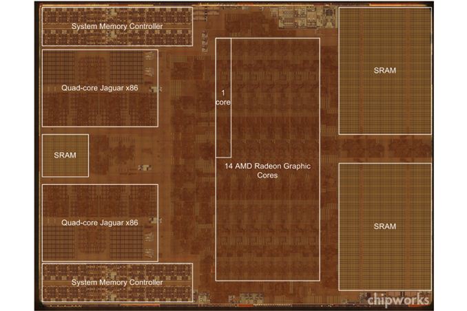
In our mini-review of the Xbox One I speculated that the shipping version of Microsoft's console featured 14 AMD GCN CUs (Graphics Core Next Compute Units), with two disabled to improve yields. Microsoft publicly stated that Xbox One development kits featured 14 CUs and Sony similarly had 20 CUs with only 18 enabled with the PS4. With Xbox One hardware in the wild, Chipworks went to task delayering the SoC/APU and confirmed the speculation - the Xbox One does indeed feature 14 CUs (pictured above).
Microsoft claims it weighed the benefits of running 12 CUs (768 cores) at 853MHz vs. 14 CUs (896 cores) at 800MHz and decided on the former. Given that the Xbox One APU only features 16 ROPs and ROP performance scales with clock speed, Microsoft likely made the right decision. Thermal and yield limits likely kept Microsoft from doing both - enabling all CUs and running them at a higher frequency. Chances are that over time Microsoft will phase out the extra CUs, although it may take a while to get there. I'm not sure if we'll see either company move to 20nm, they may wait until 14/16nm in order to realize real area/cost savings which would mean at least another year of shipping 14/20 CU parts at 28nm.
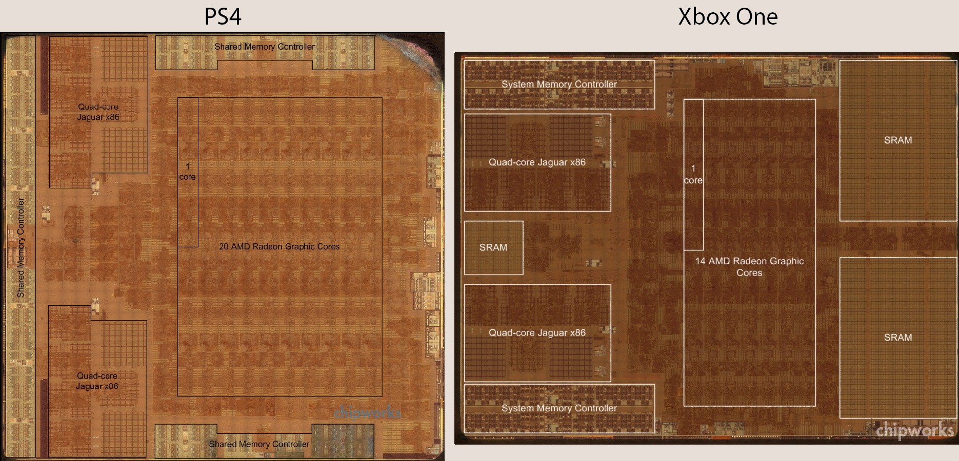
Compared to the PS4's APU, we see a very similar layout. The on-die SRAM sits next to the GPU array, and far away from the CPU, which makes sense given that the latter isn't allowed direct access to the eSRAM. You can very clearly see the tradeoff Microsoft had to make in order to accommodate its eSRAM. The GPU area shrinks considerably.


47 Comments
View All Comments
tipoo - Tuesday, November 26, 2013 - link
Yep, that eSRAM sure does take up a lot of space that could have been used elsewhere, if the main memory bandwidth didn't necessitate the eSRAM. Weird, one pool of eSRAM is too far from the GPU logic to be useful, and is right between the two CPU core clusters, what's that for?tipoo - Tuesday, November 26, 2013 - link
I also don't like how they call a compute unit a core here, as individual shaders are also called cores, which could cause confusion. Already had a few people ask why they have 12-18 cores when PC GPUs have hundreds, haha.dylan522p - Tuesday, November 26, 2013 - link
Which is why Anand did this. "2 CUs (768 cores) at 853MHz vs. 14 CUs (896 cores)"tipoo - Tuesday, November 26, 2013 - link
I know, I appreciate that. My "they" was chipworks, though I appreciate everything they do too, it should have been labeled a CU rather than core.patrickjchase - Monday, December 2, 2013 - link
Actually GPU core-counts are hugely exaggerated, and that ChipWorks' notation is at least as accurate as the way things are marketed in the consumer space.In almost every single field except for 3D graphics, a "core" is considered be an entity that executes one or more independent instruction streams ("or more" if it happens to implement SMT/hyperthreading). A core that processes multiple *data* streams via SIMD is still counted as one core. For example, Haswell can process up to 8 32-bit data elements per AVX instruction, but it's still counted as one core.
GPUs are in fact SIMD machines, just like Haswell's AVX engine. Each "Radeon Graphics Core" in XBone or PS4 executes one instruction stream. The fact that each such instruction is applied to 64 data elements in parallel does not make it "64 cores" any more than AVX support makes a single Haswell "8 cores".
There a [weak] counterargument here: GPU's have a trick that AVX doesn't (yet), namely the ability to *emulate* multiple instruction streams via vector predicates. What this means is that the entire vector engine executes the same instruction stream, but individual lanes can be selectively enabled/disabled. This allows divergent execution (different lanes appear to execute different code) though at a huge performance cost since every lane in a GPU core has to execute every instruction that any lane requires. Most people other than GPU manufacturers would say that's not sufficient to qualify the lanes as independent cores.
Short summary: ChipWorks has it right. Anand probably knows that as well as I do, but used the more common "marketing notation" to avoid confusing his readers.
SetiroN - Wednesday, November 27, 2013 - link
Because it's intuitive enough to anyone who reads chipworks.tipoo - Thursday, November 28, 2013 - link
More clueless people look at Chipworks images than you would think, lol. It was huge on the PS4 subreddit, blogs of all sorts, etc.Kevin G - Wednesday, November 27, 2013 - link
My guess would be some logic for coherency. There are two CPU clusters, a GPU, audio DSP's and other IO that all have a need to be coherent with at least one other part of the system.Another idea would be memory for exclusive usage by the system's hypervisor and/or DRM.
I don't think that it'd be a L3 cache as Jaguar uses inclusive caches in a quad core cluster. Scaling to eight cores have to have an L3 cache more than twice the size of a cluster's L2 cache.
tipoo - Wednesday, November 27, 2013 - link
Perhaps, but the PS4 seems to lack such an area for SRAM outside of the CPU caches, it must be something the One has that the PS4 doesn't, as if it was for coherency wouldn't both need it?dylan522p - Tuesday, November 26, 2013 - link
Are we ever gonna get a write up on Kings Landing? I have been reading tons about it and think I know most of what Intel showed off and understand it, but I wish you guys did one.