Intel-Micron Share Additional Details of Their 3D NAND
by Kristian Vättö on March 26, 2015 2:20 PM EST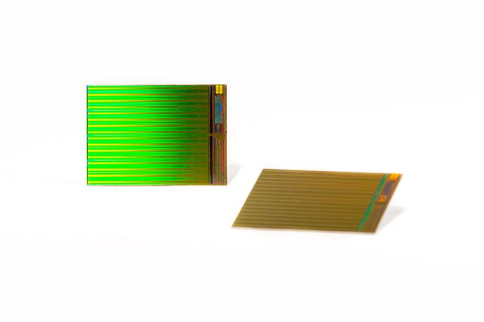
Today must be the busiest day in the world of NAND. Earlier today, Toshiba announced that it has begun sampling of its 48-layer 128Gbit 3D NAND part and now a few hours later Intel and Micron held a joint webinar that revealed a few new details about the companies' 3D NAND process. Intel-Micron originally unveiled their 3D NAND in November last year and disclosed that the first generation product will be a 32-layer 256Gbit (32GB) MLC part, which can also operate in TLC mode to bring the capacity per die to 384Gbit (48GB).
The initial part will be a 4-plane design, which is necessary for retaining high performance at such a high die capacity. For understanding why the number of planes is important, I suggest you read this page from our Crucial M550 review, but in short the number of planes translates to the number of pages that can be programmed in tandem within a single die (i.e. one page can be programmed in one plane at a time, so that's four simultaneous page programs in a 4-plane die). There's some additional latency from multi-plane programming, but with a 4-plane design you can get roughly two times the write (and read/erase too) throughput compared to a 2-plane design. That's a vital element because as the die capacity increases, less die is required to build a drive with fixed capacity (e.g. with 256Gbit die, a 256GB SSD only consists of eight dies, whereas with a 128Gbit die there would be 16 dies operating in parallel).

As I thoroughly explained in our Samsung 850 Pro review, one of the key issues with planar NAND is the shrinking number of electrons. Because 3D NAND can utilize a much larger cell structure due to the fact that scaling is done vertically rather than horizontally, the number of electrons is considerably higher, which improves both endurance and performance. The slide Intel and Micron shared shows that their 3D NAND will have roughly the same number of electrons as their 50nm process did (or actually slightly more), which is over a tenfold improvement compared to the latest 16nm node. The companies weren't willing to share the exact lithography that's used for manufacturing, but I was told that the process relies on single patterning and thus I would estimate the lithography to be somewhere between 35nm and 50nm given the limits of argon fluoride patterning. Ultimately the lithography on its own is rather useless anyway because it only measures the smallest pitch in the die and there's more than a couple of pitches that need to be known for any accurate analysis.
In terms of endurance, Micron told me that the parts will initially be rated at 3,000 P/E cycles. That may sound low, but Micron explained that the reason behind this is that all Micron's client-grade MLC has been rated at 3,000 for several years now and frankly that's more than enough for client applications. Both companies are confident that their 3D NAND technology is capable of delivering far more than that, but as validation takes time and money the first batch won't be rated at more than 3,000 cycles. It will be interesting to see what the enterprise-focused 3D NAND is rated at once it arrives to the market, but given the increased number of electrons and other endurance improvements it's safe to assume that Intel-Micron's 3D NAND will be capable of +10,000 P/E cycles as the process matures.
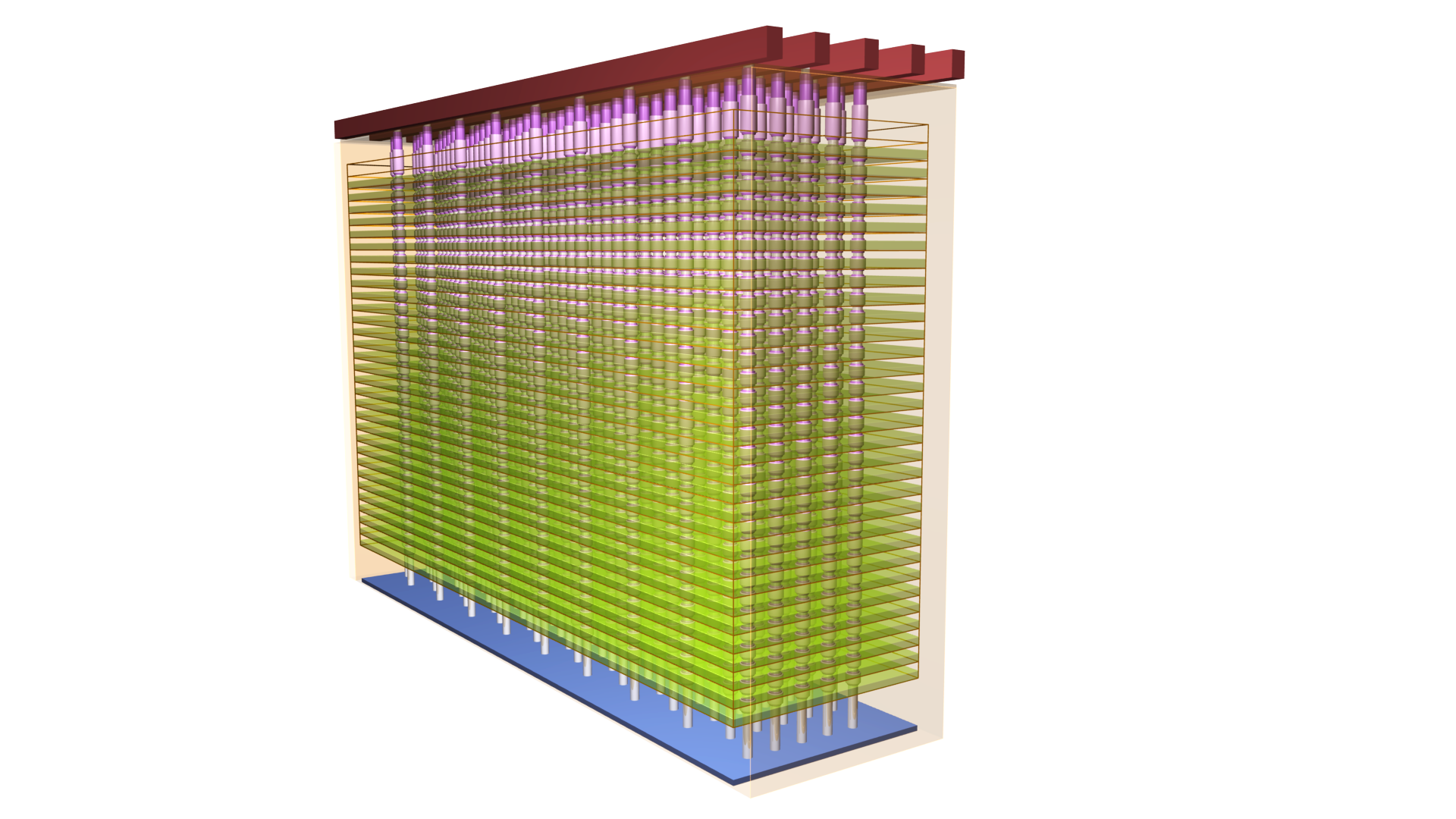
The companies also shared some high-level details of their 3D NAND structure, which has remained a secret until now. To be honest, the above illustration I was given is far from easy to understand (even the Intel/Micron engineers I talked had trouble understanding it), but what I was able to understand is that the purple tubes are the channels and the individual cells are between the channels and the green wordline (i.e. the actual cells are not really shown in the picture). Obviously, the graphs leave many questions unanswered (like how a single cell is accessed and where and how the wordlines are connected), so we'll have to wait for further details before we can fully understand how the structure differs from Samsung's and Toshiba-SanDisk's.
That said, Intel-Micron did disclose that their design utilizes a traditional floating gate, whereas the other 3D NAND designs we have seen use a newer charge trap technology. There's inherently several benefits to charge trap (e.g. less electron leakage), but Intel and Micron told me that they decided to use floating gate because it's a decades old design and the physics are well known, while charge trap is much newer and more unproven. It's impossible to outright say that one cell structure is better than the other because in the end it all boils down to cost where floating gate design is probably more cost efficient for Intel-Micron given their deep knowledge of its functionality.
All in all, we now know a few more bits about Intel-Micron's 3D NAND, but there's still lots of details to be unveiled and investigated to fully understand the differences to other 3D NAND technologies. 256Gbit MLC samples are now shipping to select customers and mass production will begin in the second half of this year, so the first products with Intel-Micron 3D NAND will likely hit the shelves in the first half of 2016.


34 Comments
View All Comments
blanarahul - Thursday, March 26, 2015 - link
I think Intel is preparing for 3D processors.blanarahul - Thursday, March 26, 2015 - link
I read somewhere that Intel has no plans to go below 10 NM on processor side of things so they will look into silicon stacking. I guess they are doing stacked floating gate NAND to prepare for that.JKflipflop98 - Saturday, March 28, 2015 - link
I can assure you we have plans to go below 10nm. You heard wrong.jjj - Thursday, March 26, 2015 - link
lol how?It's one thing to have simple repetitive structures and go 3D and quite another to have a very complex SoC.
Would be amazing if someone could do 3D GPUs (those at least have thousands of cores) but no clue if even that is in any way doable.
Morawka - Thursday, March 26, 2015 - link
can you imagine the yeilds.. 4 out of 5 layers turned out good, we are gonna have to make this a i5.they are going to have to invent ways to propagate heat vertically if 3d gpu/cpu are gonna become a thing..
ptmmac - Sunday, March 29, 2015 - link
This is purely speculation, but the move to 3 d layers may make FPG's more important for the chip design. Layering in hundreds of layers may require more ability to program around the flawed area's of the chip. Having FPG's integrated into the stack could allow them to reroute around broken or flawed areas on the chip. The downside for FPG's has been the slower process until Intel started selling their best process to companies that produce chips that don't compete with x86 chips.FPG's are also slow to change in comparison to preset silicon like current Intel CPU's. I would expect integrating them into the processor from the begining would be no small engineering feat, but compared to continuing to shrink die sizes it may be much easier.
bji - Thursday, March 26, 2015 - link
How do they make the dies for 3d NAND? My understanding of process tech is not strong, I thought that they did lithography on the face of a silicon wafer. How do they create structures deeply embedded within silicon for 3d NAND?jjj - Thursday, March 26, 2015 - link
Maybe try reading this, it's not about NAND but will give you an idea how complicated all is.http://www.anandtech.com/show/8223/an-introduction...Or just look at this pic from that article http://images.anandtech.com/doci/8223/550px-Cmos-c...
For NAND not ideal for what you are asking but this article mentions the review for the Samsung 850 Pro and it would help you understand http://www.anandtech.com/show/8216/samsung-ssd-850...
jjj - Thursday, March 26, 2015 - link
You can also have a look here http://www.chipworks.com/en/technical-competitive-...Vatharian - Thursday, March 26, 2015 - link
I know, how compilicated current SoC designs are. 8-10 layers of interconnects and parts are norm. But 32 layers of NAND, which are themselves 3D structures now (3-4 layers of components for each NAND layer, I'm guessing), ups this to over 100+ component layers. This makes actual litography process longer, and errors stack. Yields HAVE to go down, unless Samsung has way of laying down large part or all of layers at once.