Semiconductors
One of the core challenges that Rapidus will face when it kicks off volume production of chips on its 2nm-class process technology in 2027 is lining up customers. With Intel, Samsung, and TSMC all slated to offer their own 2nm-class nodes by that time, Rapidus will need some kind of advantage to attract customers away from its more established rivals. To that end, the company thinks they've found their edge: fully automated packaging that will allow for shorter chip lead times than manned packaging operations. In an interview with Nikkei, Rapidus' president, Atsuyoshi Koike, outlined the company's vision to use advanced packaging as a competitive edge for the new fab. The Hokkaido facility, which is currently under construction and is expecting to begin equipment installation...
Intel to Acquire Tower Semiconductor for $5.4B To Expand IFS Capabilities
Continuing their recent spending spree in expanding their foundry capabilities, Intel this morning has announced that it has struck a deal to acquire specialty foundry Tower Semiconductor for $5.4...
7 by Ryan Smith on 2/15/2022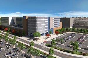
Intel Announces Ohio Fab Complex: 2 New Fabs For $20B, And Space For More
With fab expansions on tap across the entire semiconductor industry, Intel today is laying out their own plans for significantly increasing their production capacity by announcing their intention to...
114 by Ryan Smith on 1/21/2022
AMD and GlobalFoundries Wafer Supply Agreement Updated Once More: Now $2.1B Through 2025
In a short note published by AMD this afternoon as part of an 8-K filing with the US Securities and Exchange Commission, AMD is disclosing that the company has...
71 by Ryan Smith on 12/23/2021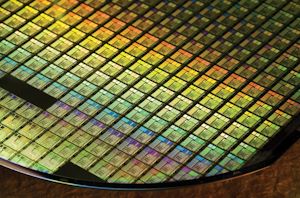
TSMC Unveils N4X Node: Extreme High-Performance at High Voltages
TSMC this week announced a new fabrication process that is tailored specifically for high-performance computing (HPC) products. N4X promises to combine transistor density and design rules of TSMC's N5-family...
42 by Anton Shilov on 12/17/2021
Semi CapEx to Hit $152 Billion in 2021 as Market on Track for $2 Trillion by 2035
Semiconductor makers have drastically increased their capital expenditures (CapEx) this year in response to unprecedented demand for chips that is going to last for years. Now the CEO of...
8 by Anton Shilov on 12/17/2021
Texas To Get Multiple New Fabs as Samsung and TI to Spend $47 Billion on New Facilities
After a year of searching for the right place of its new U.S. fab, Samsung this week announced that it would build a fab near Taylor, Texas. The company...
135 by Anton Shilov on 11/24/2021
TSMC Roadmap Update: 3nm in Q1 2023, 3nm Enhanced in 2024, 2nm in 2025
TSMC has introduced a brand-new manufacturing technology roughly every two years over the past decade. Yet as the complexity of developing new fabrication processes is compounding, it is getting...
32 by Anton Shilov on 10/18/2021
GlobalFoundries To Spend Billions: Doubling Fab 8, Creating New Fab in NY
Today at a private GlobalFoundies event, CEO Tom Caulfield accompanied by Senate Majority Leader Chuck Schumer, announced that the company is set on expansion. At the heart of this...
75 by Dr. Ian Cutress on 7/19/2021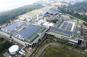
GlobalFoundries To Build New 450K Wafer-per-Year Fab in Singapore
Looking to capitalize on the ongoing chip crunch, GlobalFoundries this morning is announcing that the company is building a new chip fab in Singapore, with the groundbreaking taking place...
5 by Ryan Smith on 6/22/2021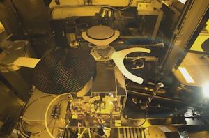
TSMC Manufacturing Update: N6 to Match N7 Output by EOY, N5 Ramping Faster, Better Yields Than N7
As part of a regular TSMC Technology Symposium, the foundry published updates on its status on it’s current leading-edge manufacturing technologies, the N7, N5 and their respective derivatives such...
50 by Andrei Frumusanu on 6/1/2021
AMD and GlobalFoundries Update Wafer Supply Agreement: Orders Through 2024, Now Non-Exclusive
In a brief Securities and Exchange Commission Form 8-K filing, AMD this afternoon has revealed that it has once again amended its wafer supply agreement with US fab (and...
41 by Ryan Smith on 5/13/2021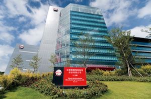
TSMC Update: 2nm in Development, 3nm and 4nm on Track for 2022
For TSMC, being the world's largest foundry with nearly 500 customers has its peculiarities. On the one hand, the company can serve almost any client with almost any requirements...
74 by Anton Shilov on 4/26/2021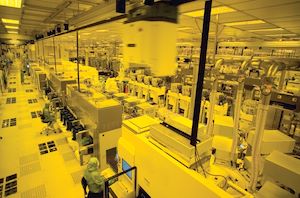
Sales of Fab Tools Surge to Over $71 Billion in 2020
SEMI, an organization representing chipmakers and producers of semiconductor production tools, published this week that sales of wafer processing equipment has surged to an all-time record of $71.19 billion...
18 by Anton Shilov on 4/15/2021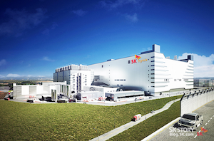
SK Hynix to Build $106 Billion Fab Cluster: 800,000 Wafer Starts a Month
Capping off a busy week for fab-related news, South Korea authorities this week gave SK Hynix a green light to build a new, 120 trillion won ($106.35 billion) fab...
41 by Anton Shilov on 4/2/2021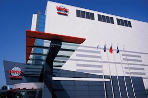
TSMC to Spend $100B on Fabs and R&D Over Next Three Years: 2nm, Arizona Fab & More
TSMC this week has announced plans to spend $100 billion on new production facilities as well as R&D over the next three years. The world's largest contract maker of...
45 by Anton Shilov on 4/2/2021
EUV Pellicles Ready For Fabs, Expected to Boost Chip Yields and Sizes
Foundries started limited usage of extreme ultraviolet (EUV) lithography for high-volume manufacturing (HVM) of chips in 2019. At the time, ASML's Twinscan NXE scanners were good enough for production...
35 by Anton Shilov on 3/31/2021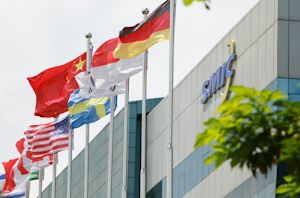
SMIC to Build a New 28nm Fab in Shenzhen: Production to Start in 2022
As further evidence that the ongoing chip crunch is hitting every level of the chip manufacturing chain, Chinese chipmaker SMIC has announced plans to build a new 28nm manufacturing...
12 by Anton Shilov on 3/20/2021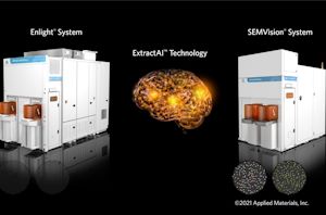
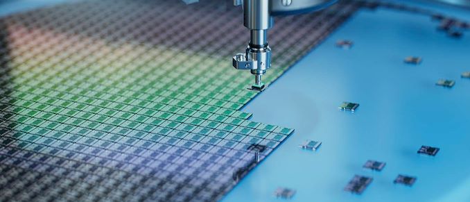
AI Meets Chipmaking: Applied Materials Incorporates AI In Wafer Inspection Process
Advanced system-on-chip designs are extremely complex in terms of transistor count and are hard to build using the latest fabrication processes. In a bid to make production of next-generation...
11 by Anton Shilov on 3/19/2021
GlobalFoundries to Invest $1.4B in Expansion, Potential Earlier IPO
GlobalFoundries this week reiterated plans to invest $1.4 billion this year in expansion of its manufacturing capacities across the world. Around one third of the sum will be co-invested...
21 by Anton Shilov on 3/4/2021
Report: Semi Demand 30% Above Supply, 20% Year-on-Year Growth
Semiconductor foundry offerings are thriving due to unprecedented demand for semiconductors and processors in recent quarters. Analysts from TrendForce believe that in Q1 2021 foundries will increase their revenue...
31 by Anton Shilov on 2/25/2021


